Universal Auto Insertion Machine J11 (8223) controller troubleshooting guide

Document part number 43380001

Revision E

Title 8223 troubleshooting guide

Date February 27, 1996

Engineer R. Lindaman

1 INTRODUCTION

The intention of this guide is to provide a method of diagnosing a problem with a 8223 controller. Due to the close interaction of the controller with the machine it is embedded in, it is often difficult to determine the cause of a problem. Therefore items such as power supplies and cabling are important.

Knowledge of ODT (Digital Equipment Corporations Online Debugging Technique) is essential. See end of guide for command summary.

2 QUICK CHECK LIST

The following are problems that have been observed in the past and should be checked first.

2.1 Power supply voltage must be set between 4.95 and 5.00 volts as measured on J11 ( put meter across C79 on CPU board ). Note the test points on the EMI/PS board do not accurately reflect the supply voltage. See section CONTROLLER POWER, subsection EMI/PS and Appendix A.

2.2 Intermittent power supply connections at rear of DC supply chassis. In particular the 3PL “RED BRICK” style connector which supplies +5,+15,15 volts to the J11 and I/O box. It’s on the rear of the power supply chassis. Due to poor connections at 3PL the J11 receives a low +5 volts. This is applicable to older machines.

2.3 Intermittent or poor connections of power cable to back of I/O box. Cause low voltage to I/O box and J11. This is applicable to older machines. Check the backplane of the I/O box. If there is a small PCB part number 433993xx MIB PWR ASSY, then the connector issues stated above should not be a problem.

2.4 On the J11 CPU board and memory expansion board some IC’s installed in sockets have bent leads. In particular IC19 on the memory expansion board is suspect.

2.5 Open fuses in the memory battery circuit ( 1FU on memory expansion board and 2FU on the J11 CPU board ). J11 CPU part number 433797xx and J11 EXP MEM 43423001 do not have a fuse!

2.6 On the memory expansion board where the battery solders to the PCB there have been bad connections. With an ohm meter the resistance between the negative battery lead and ground ( ground may be any memory IC pin 14 ) it should be a short ( less than 0.1 ohms ).

2.7 A change was made to the EMI/PS board to correct some power down problems. The machine should have a 41693302 PC CD, EMI/PS ASSY as opposed to a 41693301 ( or other ?).

2.8 System powers up properly only every other time ?. Check cable between EMI/PS and J11 CPU board ( 10 wire shielded flat cable ).

2.9 Exec’s 417247xx REV B and 405912xx, 405913xx REV L have a known power down problem. A power fail modified J11 or new exec will fix it.

2.10 If serial communications problem Check IC65, IC66, IC67. The receiver (IC67) is damaged easily by ESD. Some versions have sockets for these ICs making them easy to replace.

2.10.1 IC65 MC1488 or equivalent

2.10.2 IC66 MC3487, 26LS31C or equivalent

2.10.3 IC67 MC3486, 26LS32A or equivalent

2.11 Check jumper configuration against machine documentation.

2.12 Unit goes into ODT and will not properly accept input from the console. IC’s 43 and/or 52 may have failed. See section on IC42 and IC53 for additional information (pre 1990 units)

3 SYMPTOMS

The following are general categories of system failure.

3.1 No communications with console.

3.2 Improper communications with console

3.3 Incorrect communications with console

3.4 Fails to communicate with Host.

3.5 Trap errors.

3.6 Fails to power up in Executive program.

3.7 Losses pattern data

3.8 Incorrect control of machine I/O.

3.9 Repeats outputting the UIC restart message

4 NO COMMUNICATIONS WITH CONSOLE.

4.1 Check controller power. If OK then do next check.

4.2 Check state of J11 CPU PCB’s indicators. If OK then do next check.

4.3 Check console serial I/O.

5 IMPROPER COMMUNICATIONS WITH CONSOLE.

5.1 Check controller power. If OK then do next check.

5.2 Check IC43 and IC52. If OK then do next check.

5.3 Check console serial I/O

6 FAILS TO COMMUNICATE WITH HOST OR OTHER SERIAL I/O

6.1 Check controller power. If OK then do next check.

6.2 Check state of J11 CPU PCB’s indicators. If OK then do next check.

6.3 Check serial I/O

7 TRAP ERRORS

There are two causes of trap errors, hardware failures and software failures. Traps occur due to the program not executing properly which could be a software programming error contents of memory changing or memory failure. Hardware problems will be covered.

The following should be examined in the order given:

7.1 Check controller power. If OK then next step.

7.2 Check memory voltage supply circuit. If OK then next step.

7.3 Check EMI/PS for power timing. If OK then next step

7.4 Check Socketed IC’s. If OK then next step.

7.5 Check memory using PFAIL program.

8 FAILS TO POWER UP IN EXEC PROGRAM.

The causes for this are usually the same as those for trap errors. Follow the procedure for trap errors. Also check IC43 and IC52.

9 LOOSES PATTERN DATA

The causes for this are usually the same as those for trap errors. Follow the procedure for trap errors.

10 INCORRECT CONTROL OF MACHINE I/O

Typically these symptoms are chattering valves, improper DAC outputs, improper encoder values.

The following should be checked:

10.1 Check controller power. If OK then next step.

10.2 Check local I/O

10.3 Check external I/O

11 REPEATS OUTPUTTING THE UIC RESTART MESSAGE

This problem has been observed as being related to controller power. If the + 5 volts at the EMI/PS card is close to the limits at which it detects voltage out of tolerance, this problem can occur. Typically the EMI/PS detects under voltage when below 4.70 volts and over voltage at 5.3 volts. When the voltage is near these limits the system will Reset/Restart as the voltage drifts up and or down slightly.

The PINT indicator on the EMI/PS will activate if this is occurring. See section CONTROLLER POWER, sub section PINT INDICATOR.

11.1 Check controller power

12 CONTROLLER POWER

The following are areas to investigate regarding checking the power that the controller receives from the machine.

12.1 Supply Voltages

Measure power supply voltages at the point indicated. Variations from this should be investigated and corrected. Also see appendix A for additional information.

12.1.1 +5 Volts – The 5 volt test point should not be used for measuring the 5 volts. ( see section on CPU power, subsection EMI/PS ). Measure using one of the following, the voltage should be +4.90 to +5.00 ( VDC ).

12.1.1.1 MIB PWR Adaptor If a MIB PWR adaptor card is installed on the backplane use the Black test point on it ( +5 volt TP ) and the Yellow Ground.
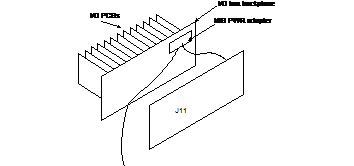
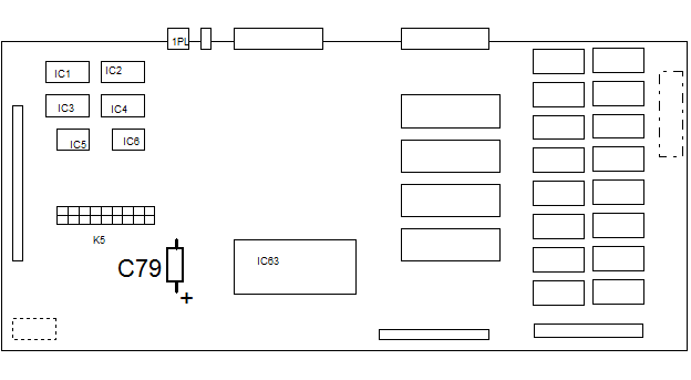
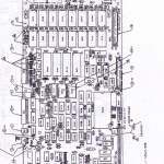
12.1.1.2 C79 On CPU Board – See Diagram no. 1 at the end of this guide for location of C79. When using this point to measure compare this voltage to the 5 volts measured on the I/O box backplane ( use pin 80 for +5 volts and pin 76 for ground ). The difference should be less than 0.1 volts. If it is not less than 0.1 volts then the “Y” adaptor cable that provides power to the I/O box and J11 should be checked for poor connections.
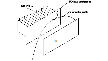
12.1.2 +15 Volts The test points on the MIB PWR adaptor card or EMI/PS board may be used. Brown test point, +14.6 to +15.00 ( VDC )

12.1.3 15 Volts The test points on the MIB PWR adaptor card or EMI/PS board may be used. Red test point, 14.6 to 15.00 ( VDC )

12.1.4 24VAC Use TP4 ( Orange ) on the EMI/PS, 20.0 to 28.0 ( VAC ). The 24 VAC comes through the shielded ribbon cable between the EMI/PS and J11 cpu board then through a fuse on the J11 cpu board then out 9PL of the J11. Check this path if there is no 24 VAC.

12.1.5 General Power Supply Notes The J11 controller is tolerant of variations in the +/ 15 volts DC and 24 VAC but NOT the 5 volts DC. Should the 5 volt supply not be within stated tolerance check the voltage drop of the connector/cables leading from the supply chassis to the I/O box. To do this measure the 5 volt supply at the supply. Typically it is set at 5.5 to 5.6 volts. If the supply is within range but the TP1 does not read the correct value then the cable should be suspect. Wiggle the connectors at the supply chassis, I/O box and Y adaptor cable in back of the I/O box. These have been observed to cause problems. Check the backplane of the I/O box. If there is a small PCB part number 433993xx MIB PWR ASSY, then the connector issues stated above should not be a problem. The DCOK indicator ON the EMI/PS should be on with the supplies are set properly. If the supplies are OK and the DCOK indicators is out the replace EMI/PS board.

12.2 CPU Power – Measure +5 on the J11 controller PCB. Measure at C79. See Diagram no. 1 at the end of this guide for location of C79. Measure +/ 15 on the J11 CPU board.

12.3 EMI/PS

The EMI/PS board ( 41693302 REV A or earlier ) has a voltage drop in the +5 volts between the I/O box side of the board and the test point side. When the test points are used to set the +5 volts ( as has been recommended ) the voltage at the I/O Box can be up to 0.25 volts more. To allow for more accurate setting of the voltage a change has been issued to reduce the voltage drop. 41693302 REV B boards have this change included.

12.4 PINT Indicator

The PINT ( Power INTerrupt ) indicator on the EMI/PS board indicates that the power detector section of the EMI/PS board has detected a interruption of the AC line or a out of tolerance condition of the 5 volt power.

On power up ( assuming power has been off for approximately 15 seconds ) the indicator should be off. Following a normal power up the indicator will stay off until a interruption of the AC line or a out of tolerance condition of the 5 volt power is detected.

This may be simulated by quickly turning the AC power off then on again. If the indicator is on it may be turned off by either turning power off for more than 15 seconds and turning on again or by pressing the small pushbutton on the EMI/PS board.

13 CPU INDICATORS

There are four CPU indicators. Providing that system power is OK then the indicators have the following meaning.

13.1 All On

When all LED’s are on it generally means that the cpu is being held in reset. This may be due to:

13.1.1 System power incorrect ( see section on supply voltages )

13.1.2 Bad EMI/PS board. ON EMI/PS measure IC40 pin 3 it should be High (4.0 to 5.1 volts ) and the anode of D5 should measure 10 to 15 volts. If these are incorrect then probably the EMI/PS is bad.

13.1.3 Bad cable between EMI/PS. If the voltages at the EMI card are OK then proceed to check these voltages at the J11 board. ON the J11 board measure IC34 pin 5, should be high 4.0 to 5.1 volts. Measure R18 ( side closest to 9PL ), it should be 10 to 15 volts. If these are incorrect and the EMI was OK then the cable is bad. If these ar OK then the J11 CPU board is bad.

13.1.4 Bad J11 CPU board. The measurements stated on bad cable between EMI/PS and J11 should indicated if J11 is OK.

13.1.4.1 See section on IC17

13.2 LT1 On, Others Off – This is the normal mode of operation. LT1 on indicates the system is running a program ( only true when LT24 are off ).

13.3 All Off – This indicates that the unit is in ODT mode. This is a normal mode of operation.

13.4 Other Combinations – Other combinations of indicators on/off general indicate the CPU has detected a hardware problem. The J11 CPU assy should be considered bad.

14 CONSOLE SERIAL I/O

Verify jumper configuration of K20, and K13 against system documentation ( generally 9600 baud and RS 232). The following check is for RS232. If RS 422 is used the service person should be capable of doing a similar test procedure.

14.1 If a expansion serial I/O card is installed then remove it. Put the RUN/HALT switch into HALT ( ODT ).

14.2 Put scope probe on IC67 pin 1. Press a key on the keyboard, a signal switching should be seen. If there is no signal then the cabling between the J11 and the terminal should be checked. If there is a signal then the J11 is receiving data from the terminal. The next check is to verify that the J11 transmits.

14.3 Put the scope probe on IC65 pin 3. Press a key on the keyboard. If the J11 receives data while in ODT then it should echo it out the transmitter. A switching signal should be observed on the IC pin. If there is a signal the cabling between the J11 and terminal should be checked. If there is no signal verify that the cables are not shorting the signals making it appear that the Drivers and receivers are bad. Generally if a signal is being received (IC67 pin 1) and not transmitted ( IC65 pin 3 ) then the J11 is bad.

15 SERIAL I/O

15.1 Verify jumper configuration against the documentation provided for the machine.

15.2 There are programs in ROM that assist with serial I/O diagnostics. These are labeled on the J11’s cover as ASCII DUMP and DATA ECHO.

15.3 The following apply to either the J11 CPU board or the serial expansion board.

15.4 ASCII dump will output from the serial port the ASCII character set

15.5 DATA ECHO will receive data from a port then transmit it to another.

15.6 To start the programs the user must be in ODT. In ODT enter the number given ( on the cover ) for the desired program and then G ( for GO). The program prompts for additional information.

15.7 For ASCII DUMP deposit the base address for the serial port in the register displayed, then type P for proceed. The base address for the port is given in the J11 manual. The port number must be determined from machine documentation ( Channel 1 for host, Channel 24 for verifier, etc ).

Port name Base address
Console (J1, COMM INTC ASSY) 17777560
Host (J4, COMM INTC ASSY) 17776500
Channel 2 (J2,J3 COMM INTC ASSY) 17776510
Channel 3 (J2,J3 COMM INTC ASSY) 17776520
Channel 4 (J2,J3 COMM INTC ASSY) 17776530
Channel 5 (J2,J3 COMM INTC ASSY) 17776540
Channel 6 (J2,J3 COMM INTC ASSY) 17776550
Channel 7 (J2,J3 COMM INTC ASSY) 17776560
Channel 8 (J2,J3 COMM INTC ASSY) 17776570
Channel 9 (J2,J3 COMM INTC ASSY) 17776600
Channel 10 (J2,J3 COMM INTC ASSY) 17776610
Channel 11 (J2,J3 COMM INTC ASSY) 17776620
Channel 12 (J2,J3 COMM INTC ASSY) 17776630
Channel 13 (J2,J3 COMM INTC ASSY) 17776640
Channel 14 (J2,J3 COMM INTC ASSY) 17776650
Channel 15 (J2,J3 COMM INTC ASSY) 17776660
Channel 16 (J2,J3 COMM INTC ASSY) 17776670

15.8 For tests like ASCII dump it is suggested that the tests be started with the terminal (UCT) connected to the console port. If the test is to check one of the other ports (Host for example) it is suggested that the connectors at the COMM INTC ASSY be switched so that the output of the port under test is connected to the UCT or terminal.

15.9 For DATA ECHO deposit the two required base addresses in R0 and R1. Typically one port is the console the other the port under test.

15.10 Check the suspected ports transmitter first by running the ASCII DUMP program for the port. Observe with a scope the output of the driver IC ( RS232 or RS422 ). A switching signal should be present. If there is then the transmitter is OK. If there isn’t then remove the 40 pin ribbon cable at the PCB. If the signal is there now suspect the cabling, if there isn’t then PCB ( J11 or expansion ) is probably bad.

15.11 The receiver section is more difficult to check as a source of input is required. If possible the device connected to the port should be run to output data to the controller. With data coming in to the controller observe the input of the receiver on the PCB. If the signal is not there then check cabling. If the signal is there then the board is probably bad.

15.12 A jumper cable ( wire, clip leads, maintenance adaptor ) may be used to jumper the ports output to it’s input on the COMM INTC card. Using DATA ECHO set the output and input port to the same base address for the port being tested. The data sent out should be returned to the input. Using a scope the ports driver’s and receivers may be examined.

16 MEMORY VOLTAGE SUPPLY

The following is a check of the circuit that supplies power to the

memory IC’s.

16.1 Expansion Memory Board.

16.1.1 With system power applied, measure the voltage on IC16 pin 28 and IC12 pin 28. The voltage should be greater than 4.8 volts. If not the board is bad.

16.1.2 With system power off, measure the voltage on IC16 pin 28 and IC12 pin 28, The voltage should be greater than 3.0 volts. IF not check the fuse 1FU and the battery. If the fuse and the battery are OK but the voltage is less than 3.0 volts then the board is bad. EXP MEM board 43423001 does not have a fuse.

16.2 J11 CPU Board – The memory expansion board should be removed to do this check. Data stored in the system will be lost when removing the expansion board.

16.2.1 With system power applied, measure the voltage on IC101 pin 28 and IC97 pin 28. The voltage should be greater than 4.8 volts. If not the board is bad.

16.2.2 With system power off, measure the voltage on IC101 pin 28 and IC97 pin 28, The voltage should be greater than 3.0 volts. IF not check the fuse 2FU and the battery. If the fuse and the battery are OK but the voltage is less than 3.0 volts then the board is bad.

17 EMI/PS CIRCUIT TIMING

17.1 With system power applied examine on the J11 CPU IC34 pin 5 it should be a logic high. This is signal BPOKH. Pull out connector plug on 9PL, the signal should go low. Install the connector it should go high. If this does not happen there is a problem with either the cable between the EMI/PS and J11, the EMI/PS is bad or the system power is bad.

17.2 With system power applied examine on the J11 CPU R18 the side closest to 9PL, it should be between 15 and 10 volts. This is signal BDCOKH. Pull out connector plug on 9PL, the signal should go about 0 volts ( +/1.0 volts). Install the connector it should go low again. If this does not happen there is a problem with either the cable between the EMI/PS and J11, the EMI/PS is bad or the system power is bad.

17.3 A scope will be required to examine the timing relationship between BPOKH and BDCOKH. Sync the scope to trigger ( and display ) on BPOKH going low. With the second channel of the scope examine BDCOKH. With system power applied pull out connector 9PL. This should send BPOKH low. 2 to 4 ms later BDCOKH should go high. If this timing is incorrect then the EMI/PS board is probably bad.

18 SOCKETED IC’S

Examine IC’s that are installed in sockets both on the J11 CPU and the memory expansion board. On some expansion boards IC19 is installed in a socket although it may not appear that way. EXP MEM PCB part number 43423001 does not have a socket.

Look for leads that may have bent under the IC when the IC was installed in the socket.

19 USING PFAIL PROGRAM

The PFAIL (DA01) program performs two functions, a write/read test of memory and a fill then check test.

19.1 Load PFAIL like an EXEC. It will perform a memory size then memory test. It will the output the > prompt. Be sure to enter capital letters, some versions will not accept lower case.

19.1.1 Enter M will cause the program to enter a mode to test write/read test memory. If the memory test indicates an error the J11 is probably bad.

19.1.2 Entering P will cause the unit to fill memory with data. When answering questions to the ” P ” test enter 2 for the fill pattern, N for the Power fail memory loop and Y for the Automated test question. The program will fill memory then enter a mode where it will continually check it. Turn the system off then on again. When it powers up it should begin checking checking memory. If any data is altered the program will report the error. If the memory passes the program will print a period ( . ) then continue testing. If the program prints an error then the j11 unit is probably bad.

20 LOCAL I/O

Local I/O are the I/O located in the I/O box that the J11 is attached to.

20.1 Often a bad I/O card causes other I/O cards or the J11 to appear bad.

20.2 Often a PCB will be replaced and the problem will appear to be fixed only to have the same or similar symptom to appear later.

20.3 A problem in the local I/O box could cause symptoms of I/O problems in External I/O boxes. This is due to the data transfer to external I/O boxes going through the data lines of the local I/O box.

20.4 DTOP, DTIP and DSFx pins on the backplane are next to +/15 volt power supply pins. If these pins are shorted together failures will occur to the J11, EMI/PS and most other I/O cards. Check that cables don’t lean or push pins together. Insure the connector of the J11 that plugs into the backplane is correctly positioned before applying power. Poor alignment of I/O cards in the I/O box may cause these pins to short.

20.5 The most effective method is to use a scope and a simple test program entered in ODT. When running the test program the clock should be disabled ( Kx all jumpers in ). Be sure to return clock jumpers when finished.

20.5.1 The test program is used to continuously read or write I/O location.

20.5.2 While executing, the DSF, DTOP or DTIP and data lines should be observed.

20.5.3 If improper logic levels are observed then begin removing I/O cards until the signal becomes correct. If it does not become improved then either the J11 or EMI/PS is bad.

20.5.4 The following are the test programs.

20.5.4.1 Write loop

Using ODT enter at location 1000

1000/10037 LABEL: MOV R0,166000

1002/166000

1004/775 BR LABEL

Location 1002 is the DSF address being tested. EX DSF0 =166000, DSF1 =166002, DSF2 =166004, etc

Then enter 1000G to start the program

The DSFx DTOP should look as follows
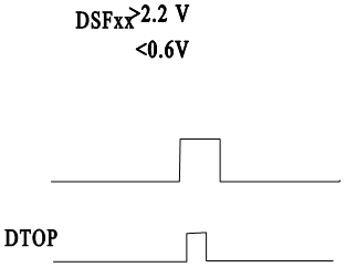
20.5.4.2 READ loop

Using ODT enter at location 1000

1000/13700 LABEL: MOV 166000,R0

1002/166000

1004/775 BR LABEL

Location 1002 is the DSF address being tested. EX DSF0 =166000, DSF1 =166002, DSF2 =166004, etc

Then enter 1000G to start the program

The DSFx DTIP should look as follows
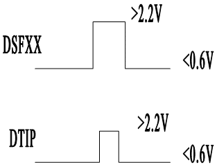
The data lines ( DIxx for read cycles and DOxx for write cycles ) should be observed during the DTOP, DTIP time. When there are problems the logic levels are usually wrong.

21 EXTERNAL I/O

External I/O are those in I/O boxes that the J11 system is not attached to the back of. Note that a problem in the local I/O box could cause symptoms indicating a problem in external I/O boxes.

A procedure similar to that of the local I/O box should be followed. Executing a write or read test program and observing the signals.

22 IC43 AND IC52

IC43 and IC52 are Signetics PLS159 IC’s. On Units having J11 CPU part numbers 4034830x, 4315450x , 4320900x , 4332990x, these parts have been failing. The typical symptoms observed are that the unit enters ODT and then will not communicate with the console properly. The space bar on the console might be entered then the unit scrolls characters off the screen. Or the controller does not understand any ODT entries.

22.1 IC43 – IC43 generates the event clock signal ( normally jumper set for IC43 1.0 ms ). When this chip fails it outputs to the data bus all the time. When this happens the microprocessor cannot read or write any data properly. A simple test is to remove the chip ( if it is in a socket ). If the controller now understands console input then this chip is the problem.

22.2 IC52 – IC52 generates timing clocks for circuits on the board including the 614Khz clock required by the serial I/O chips. When this chip fails it outputs wrong frequencies. Pin 16 of IC52 should be a square wave 614.4 Khz. If it is not then the chip is bad. Also pin 12 should a low. If it pulses high then IC52 is bad.

23 IC17

23.1 IC17 is a SN74128. It provides signals (DTOP and DTIP) to the I/O box backplane. Next to these signals on the backplane are +15 and -15 volts which can short to the DTOP and DTIP signals. When this happens IC17 is damaged. When this IC fails it will frequently cause the J11 not function or improperly function. Look for the IC to be discolored or burned. A Check of the logic levels on the pins may confirm that this part has failed. Also check that there are no jumper shunts installed across pins of connector 8PL (Header post with flexible circuit attached).

24 APPENDIX A

24.1 Setting Of Power Supply Voltages

The J11 CPU board will operate properly with voltages anywhere from 4.80 to 5.2 volts On the EMI/PS card in the I/O box there is a voltage detector that detects voltages less than 4.7 and greater than 5.3 (approx. ). When the detector senses voltages outside of this range it will issue a quick power down timing sequence to the J11. This quick power down sequence is what causes the memory data to change on controllers that do not have the power fail modifications.

To allow for maximum variation ( mostly due to connector problems ) it is suggested that the voltage be set as close to 5.00 volts as possible. This allows the voltage to drift up or down the maximum amount.

An example. Suppose the voltage is nominally set for 4.90 volts. Then the voltage drifts down 0.2 volts to 4.70 volts. The voltage detector will send the J11 through the quick power down timing cycle, possibly causing memory problems. If the voltage is set to 5.00 volts and the 0.2 volt drift occurs then the system will still operate properly because the voltage is still within the tolerance window.

25 ODT summary

Command Symbol Function
Slash n/ Opens the specified location (n) and outputs it’s contents. n is an octal number
Carriage return <CR> Closes an open location
Line Feed <LF> Closes an open location and then opens the next contiguous location.
Internal register designator $n or Rn Opens a specific processor register (n). n is and integer from 0 to 7 or the character S
Go G Starts program execution.
Proceed P Resumes execution of a program.

26 DIAGRAM NO.1

26.1 Location Of C79

Change History

1. 2/1/96 Added section on IC17.

2. 2/27/96 Deleted last senteence in section 2.3 on red brick connector. Misleading reader about looking at I/O box.
AI spare parts、Universal Parts,UIC,TDK.VCD Sequencer.SMT,THT,PCB,PCBA,AI,wave soldering,reflow oven,nozzle,feeder,wave soldering,PCB Assembly, LED, LED lamp, LED display

OUR NEW MACHINE S-7000 IN THAILAND

Southern Machinery just finish a new project in Thailand.
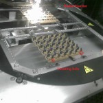
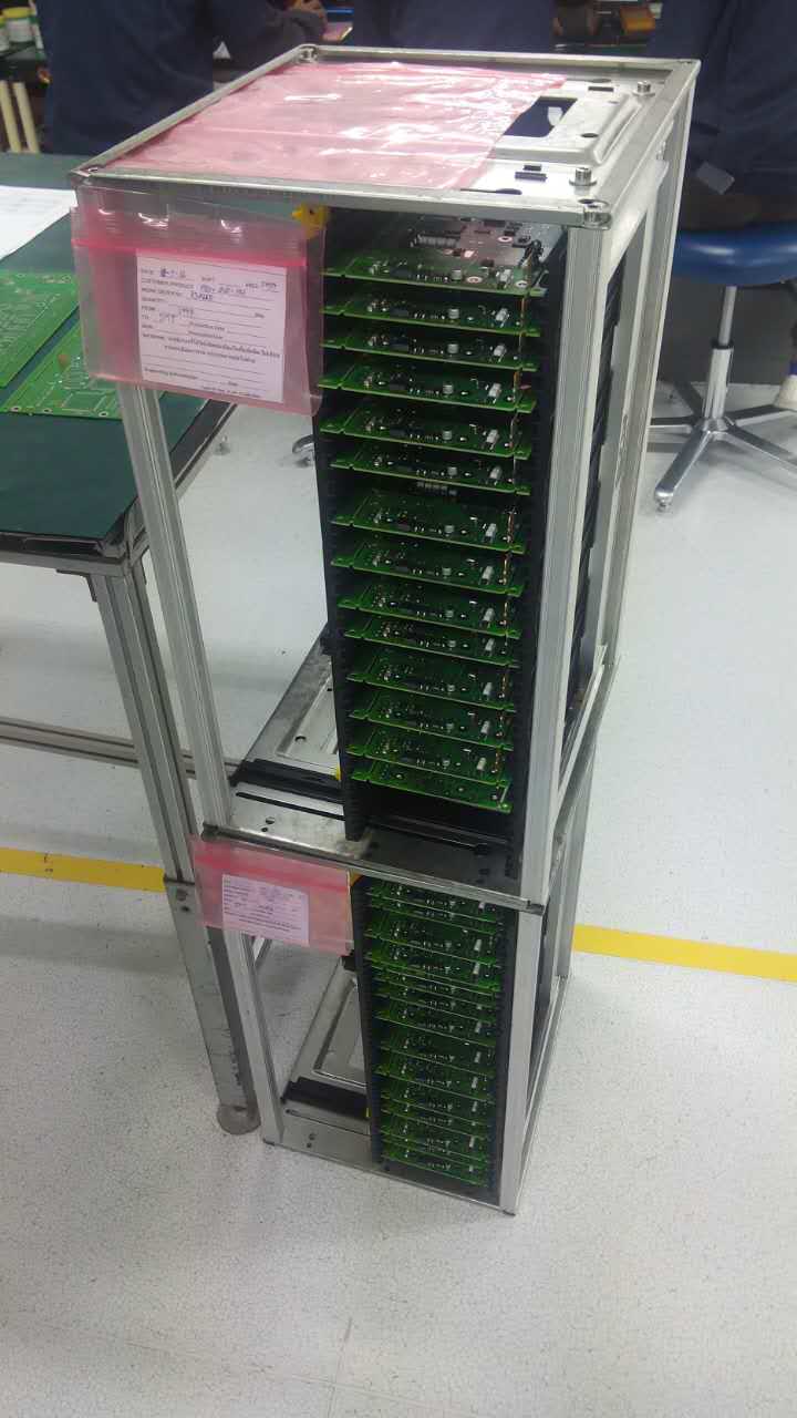
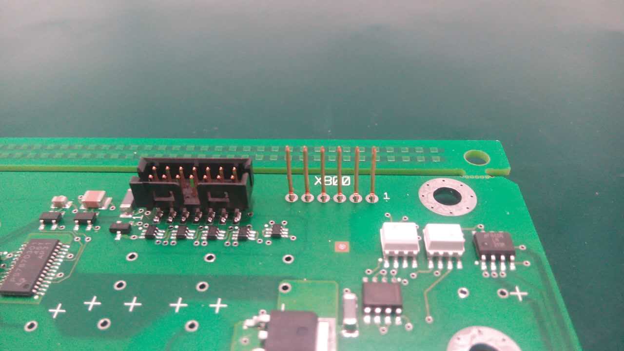
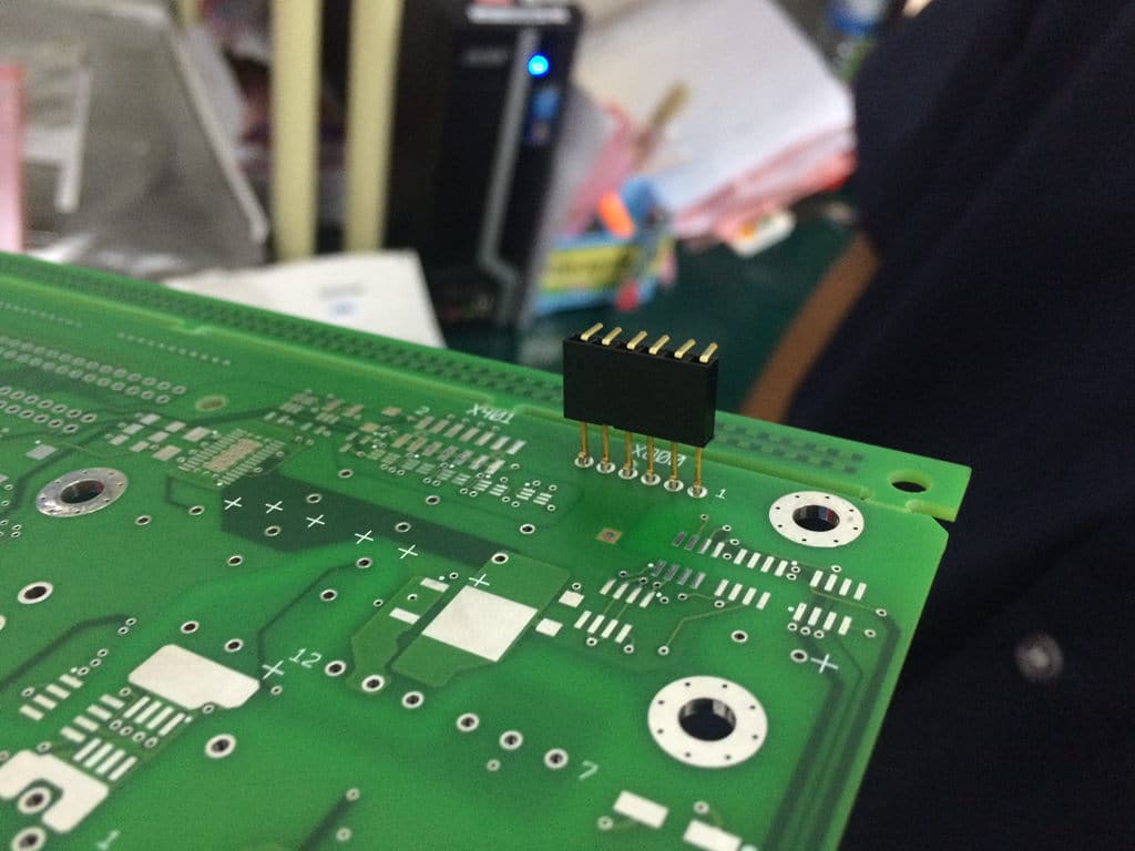
We sale a new model S-7000 to a thai customer in Samut prakan,maybe it’s the first TE square pin auto-insert machine in the world .

we send a engineer to thai for install this machine and training customer.

At last,we reach customer’s production target & quality requirements successfully

s7000 in thai

s7000-2

s7000-4

s7000-5

s7000-1

pin insert


AI spare parts、Universal Parts,UIC,TDK.VCD Sequencer.SMT,THT,PCB,PCBA,AI,wave soldering,reflow oven,nozzle,feeder,wave soldering,PCB Assembly, LED, LED lamp, LED display,

Universal Auto Insertion machine spare parts – SCREW


Nuts
42519400 Hex Nut *
42519500 Hex Jam Nut *
42519600 Hex Nut – Machine Screw HEXNUT-MS
42519700 Hex Nut – Small Pattern HEXNUT-SP
42519800 Hex Nut – Metric *
42519900 Hex Nut – Nylon HN-N
42555700 Hex Nut – Left Hand Thread HN-LHT
42520000 Square Nut – Standard SQNUT-STD
42520100 Square Machine Screw Nut SQMSNUT
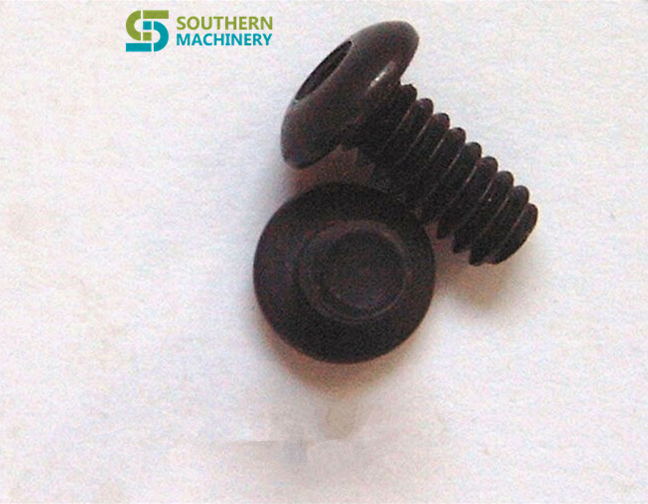
Socket Button Head Screws
42520200 Socket Button Head Screw SBHS
42520300 Socket Button Head Screw SBHS-NP
W/Nylon Patch
42520400 Metric Socket Button Head MSBHS
Screw
Hex Head Screw
42520500 Hex Head Cap Screw HHCS
42520600 Hex Head Machine Screw HHMS
42521200 Metric Hex Head Machine MHHMS
Screw
42522100 Lag Screw LAG SCR
42555300 Hex Head Cap Screw – Full HHCS-FTHD-SMHD
Thread – SMHD
Socket Head Cap Screws
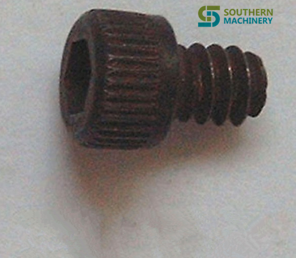
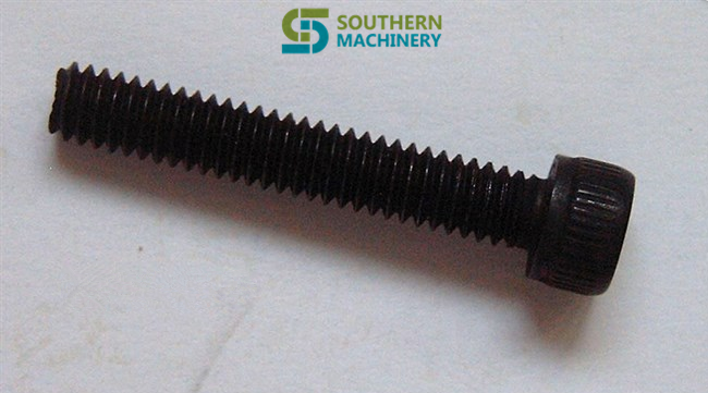
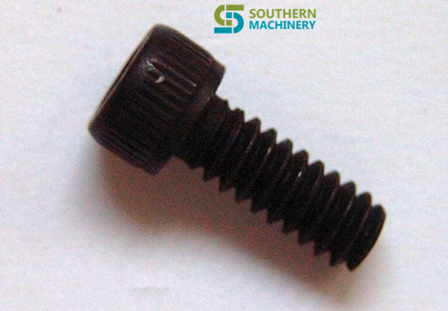
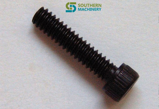
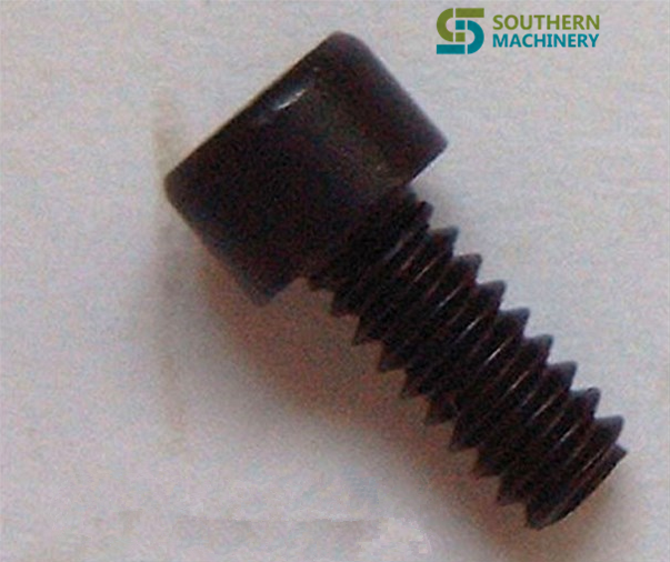
42520700 Socket Head Cap Screw SHCS
42520800 Socket Head Cap Screw SHCS-NP
W/Nylon Patch
42520900 Socket Head Cap Screw SHCS-SS
Stainless Steel
42521000 Socket Head Cap Screw SHCS-LH
Low Head
42521100 Metric Socket Head Cap MSHCS
Screw
42521300 Socket Head Cap Screw SHCS-N
Nylon
42554900 Metric Socket Low Head Cap MSLHCS
Screw
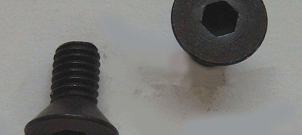
Flat Head Screws
42521400 Flat Head Machine Screw FHMS
42521500 Flat Head Wood Screw FHWS
42521600 Socket Flat Head Screw SFHS
42521700 Socket Flat Head Screw SFHS-NP
W/Nylon Patch
42521800 Metric Socket Counter Sink MSCS
Screw
42521900 Flat Head Self Tap Screw FHSTS-TA
Type – A
42522000 Slotted Flat Head Screw *
Nylon
42555400 Flat Head Thread Cutting FHTCS
Screw
42555600 Flat Head Machine Screw 100 FHMS-100 DEGREE
Counter Sunk
Pan Head Machine Screw
42522200 Pan Head Machine Screw PHMS
42522300 Pan Head Self Tapping Screw PHSTS-TA
Type-A
42522400 Pan Head Self Tapping Screw PHSTS-TF
Type-F
42522500 Metric Pan Head Machine Screw MPHMS
42522600 Pan Head Screw – Nylon PHS-N
42555000 Pan Head Self Tapping Screw PHSTS-T25
– Type 25
42555500 Pan Head Thread Cutting Screw PHTHCS
Round Head Screws
42522700 Round Head Drive Screw RHDS-TU
– Type U
42522800 Round Head Machine Screw RHMS
42522900 Round Head Wood Screw RHWS
42566000 Round Head Square Neck Bolt RHSNB
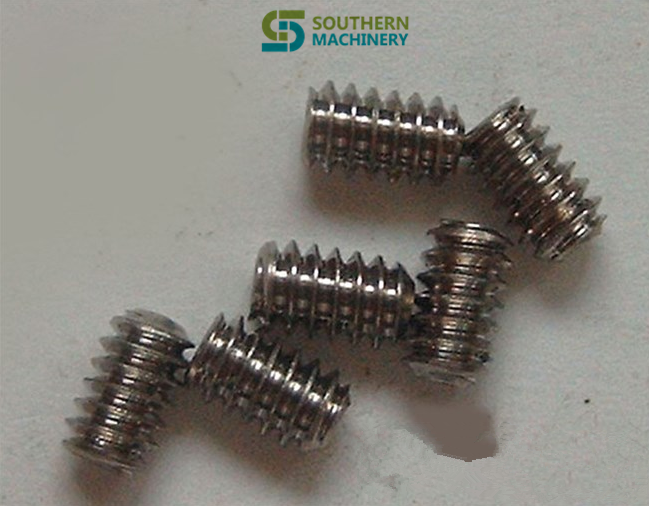
Set Screws
42523000 Socket Set Screw Cone Point SSSCNP
42523100 Socket Set Screw Cup Point SSSCPP
42523200 Socket Set Screw Cup Point SSSCPP-NP
W/Nylon Patch
42523300 Socket Set Screw Flat Point SSSFP
42523400 Socket Set Screw Half Dog Point SSSHDP
42523500 Socket Set Screw Knurl Cup Point SSSKCPP
42523600 Socket Set Screw Oval Point SSSOP
42523700 Socket Set Screw Cup Point SSSCPP-SS
Stainless Steel
42523800 Metric Socket Set Screw Cup Point MSSSCP
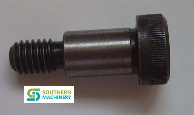
Shoulder Screws
42523900 Socket Head Shoulder Screw SHSS
42524000 Metric Socket Shoulder Screw MSSS
10463000 Shoulder Screws *
Washers
42524100 Flat Washer FW
42524200 External Tooth Lock Washer ETLW
42524300 Internal Tooth Lock Washer ITLW
42524400 Split Lock Washer SLW
42524500 Metric External Tooth Lock Washer MITL
42524600 Metric Flat Washer MFW
42524700 Flat Head External Tooth Lock FHETL
Washer
42524800 Split Lock Washer, Black SLW-BLACK
42524900 Flat Washer, Black FW-BLACK
42555100 Machine Screw Flat Washer MS-FW
Pins
42525000 Standard Dowel Pin SDP
42525100 Oversize Dowel Pin ODP
42525200 Pull Dowel PD
42525300 Dowel Pin – Pic DP-PIC
42525400 Spring Pin SPRG PIN
42525500 Taper Pin *
42525600 Metric Standard Dowel Pin MSDP
42525700 Metric Spring Pin MSP
42555200 Spirol Pin – Pic SP-PIC
Inserts
42525800 Heli-coil Insert *
AI spare parts?Universal Parts,UIC,TDK.VCD Sequencer.SMT,THT,PCB,PCBA,AI,wave soldering,reflow oven,nozzle,feeder,wave soldering,PCB Assembly, LED, LED lamp, LED display,
80011303 SCREW, SHOULDER SHSS 1.2×3.4
AI spare parts?Universal Parts,UIC,TDK.VCD Sequencer.SMT,THT,PCB,PCBA,AI,wave soldering,reflow oven,nozzle,feeder,wave soldering,PCB Assembly, LED, LED lamp, LED display,
80007204 SSSOP 1.4-20 X 3.4
AI spare parts?Universal Parts,UIC,TDK.VCD Sequencer.SMT,THT,PCB,PCBA,AI,wave soldering,reflow oven,nozzle,feeder,wave soldering,PCB Assembly, LED, LED lamp, LED display,
80004602 SSS 4-40×3.16
AI spare parts?Universal Parts,UIC,TDK.VCD Sequencer.SMT,THT,PCB,PCBA,AI,wave soldering,reflow oven,nozzle,feeder,wave soldering,PCB Assembly, LED, LED lamp, LED display,
80001301 SBHS 4-40×1.4
AI spare parts?Universal Parts,UIC,TDK.VCD Sequencer.SMT,THT,PCB,PCBA,AI,wave soldering,reflow oven,nozzle,feeder,wave soldering,PCB Assembly, LED, LED lamp, LED display,
80000109 SHCS http://buyneurontinonlinehere.com 4-40 X 1.8
AI spare parts?Universal Parts,UIC,TDK.VCD Sequencer.SMT,THT,PCB,PCBA,AI,wave soldering,reflow oven,nozzle,feeder,wave soldering,PCB Assembly, LED, LED lamp, LED display,
80000407 SHCS 8-32 X 1
AI spare parts?Universal Parts,UIC,TDK.VCD Sequencer.SMT,THT,PCB,PCBA,AI,wave soldering,reflow oven,nozzle,feeder,wave soldering,PCB Assembly, LED, LED lamp, LED display,
80013801 SPRG PIN .062 X .187
AI spare parts?Universal Parts,UIC,TDK.VCD Sequencer.SMT,THT,PCB,PCBA,AI,wave soldering,reflow oven,nozzle,feeder,wave soldering,PCB Assembly, LED, LED lamp, LED display,
80000514 SHCS 10-32 X 3.8
AI spare parts?Universal Parts,UIC,TDK.VCD Sequencer.SMT,THT,PCB,PCBA,AI,wave soldering,reflow oven,nozzle,feeder,wave soldering,PCB Assembly, LED, LED lamp, LED display,
80000302 SHCS 6-32 X 3.8
AI spare parts?Universal Parts,UIC,TDK.VCD Sequencer.SMT,THT,PCB,PCBA,AI,wave soldering,reflow oven,nozzle,feeder,wave soldering,PCB Assembly, LED, LED lamp, LED display,
80000104 SHCS 4-40 X 1.2
AI spare parts?Universal Parts,UIC,TDK.VCD Sequencer.SMT,THT,PCB,PCBA,AI,wave soldering,reflow oven,nozzle,feeder,wave soldering,PCB Assembly, LED, LED lamp, LED display,
80000102 SHCS 4-40 X 1.4


The Sights and Sounds of Normal machine Operation for Universal Auto Insertion Machine

The Sights and Sounds of Normal machine Operation

Instructional Strategy for this module

Activity: Name and Locate the Major IM8 Electrical Chassis

SINGLE HEAD IM8 MACHINES FRONT VIEW (Lower Frame)

SINGLE HEAD IM8 MACHINES REAR VIEW (Lower Frame)

Activity: Identifying the Normal Sights and Sounds of

Machine Operation

Zeroing Sequence of a VCD/SEQ 8 Machine:

Module Summary

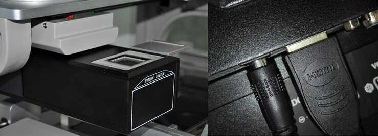
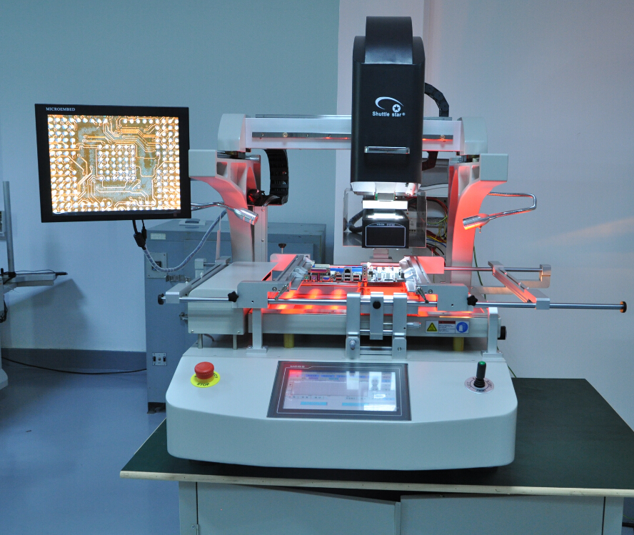
Auto pickup and placement BGA Rework station , High Precision mounting ,HDMI digital signal image SV560A

Best choice ! Auto pickup and placement BGA Rework station , High Precision mounting ,HDMI digital signal image SV560A

PCB Size W20*D20 ~ W550mm x D500mm
Workable area W550*D500mm
PCB Thickness 0.5~ 4mm
Applicable BGA 1*1~80*80mm
Working table adjustment Front/Rear ± 10mm Left/Right ± 10mm
PCB locating way Jig
placement precision ±0.01mm
Min pitch of bga ball 0.15mm
Gross power 5600W
Bottom IR Preheat 3600W
Top heater 1200W
Bottom heater 800W
MAX BGA weight 80g
Power supply Single Phase, 220VAC, 50/60 Hz
Machine dimension L750*W705*H800mm
Weight Approx 100kg

Product Description

Three temperature zone:

1) Top hot air heater

2) Bottom hot air heater

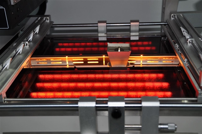
3) Bottom IR preheat – Prevent PCB board deforming ,and we use import IR wave gilding heater plate with high temperature glass,temperature increasing and decreasing rapidly ,it can protect PCB board from deformation and ensure repair effect .

Best choice ! Auto pickup and placement BGA Rework station , High Precision mounting ,HDMI digital signal image SV560A

Auto function:

auto pick-up,auto soldering,auto desoldering and auto placement function – PLC control

Best choice ! Auto pickup and placement BGA Rework station , High Precision mounting ,HDMI digital signal image SV560A

Best choice ! Auto pickup and placement BGA Rework station , High Precision mounting ,HDMI digital signal image SV560A

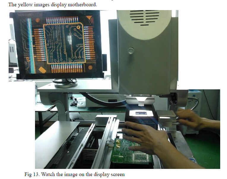
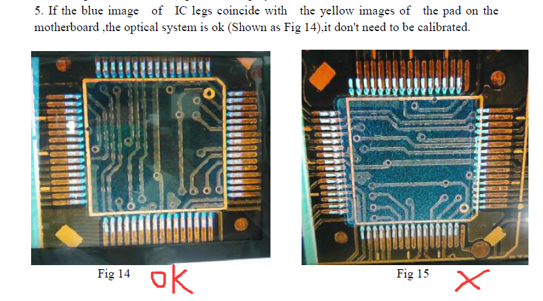
HD color optical camera system: –

1) Split vision

2) Zoom in/out and micro-adjust

3) Equipped with aberration
4) Detection device

5) With auto focus and software operation function

Best choice ! Auto pickup and placement BGA Rework station , High Precision mounting ,HDMI digital signal image SV560A

Best choice ! Auto pickup and placement BGA Rework station , High Precision mounting ,HDMI digital signal image SV560ABest choice ! Auto pickup and placement BGA Rework station , High Precision mounting ,HDMI digital signal image SV560A

The other :

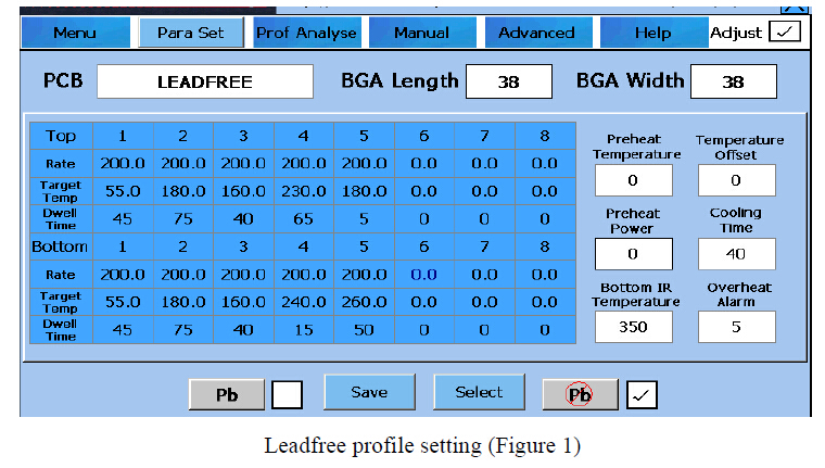
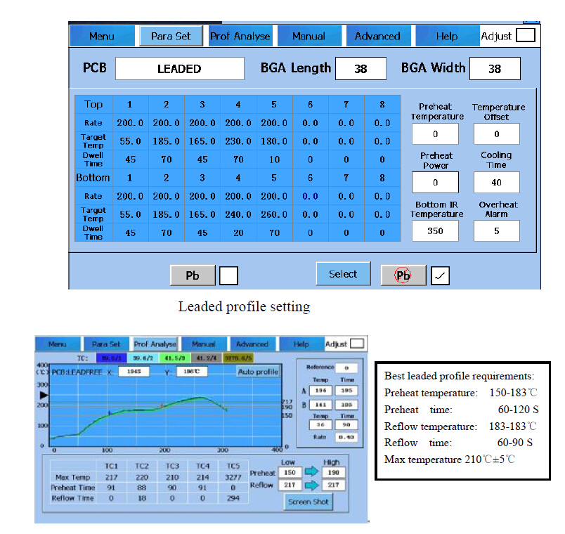
1) Embedded industrial computer, touch screen interface, real-time temperature curve display,able to display temperature curves and practical curves as the same time: can analyze the practically-tested
profile, and compare them with the history saved profiles;

Best choice ! Auto pickup and placement BGA Rework station , High Precision mounting ,HDMI digital signal image SV560A

Best choice ! Auto pickup and placement BGA Rework station , High Precision mounting ,HDMI digital signal image SV560A

2) Built-in vacuum pump, 60 °rotation in φ angle, mounting nozzle is micro-adjustable;

3) 8 segments of temperature up(down) and 8 segments constant temperature control, profile saving is
unlimited in the industrial computer;

4) Suction nozzle can identify material and mounting height automatically, and can control the air
pressure within a small range ;

Best choice ! Auto pickup and placement BGA Rework station , High Precision mounting ,HDMI digital signal image SV560A
5) Big size splint, equipped with deformation-proof supporting device, suitable for the accurate rework of all kinds of PCB;

Best choice ! Auto pickup and placement BGA Rework station , High Precision mounting ,HDMI digital signal image SV560A

Best choice ! Auto pickup and placement BGA Rework station , High Precision mounting ,HDMI digital signal image SV560A

This product has patents:

A. top heating apparatus ZL 2009 2 0262216.X utility model;

B. top heater component t ZL 2009 2 0162612.5 utility model;

C.suction nozzle device ZL 2007 2 0127185.8 utility model;

D.top heating apparatus ZL 200910238919.3 inventive patent.)

Best choice ! Auto pickup and placement BGA Rework station , High Precision mounting ,HDMI digital signal image SV560A

IM Through Put Calculator for Universal Auto Insertion

IM Through Put Calculator
Enter only fields in “Red font”
Product Description 6241F 6380B 6683C 6683D 6687C 6292C 6293C
Maximum Insertion Rate (Components per Hour) 25,000 21,000 22,500 32,500 25,000 40,000 40,000
Pattern Derate (Note 1) 5% 5% 5% 5% 5% 5% 5% (This derate is only from first insertion to last insertion on the board)
Feeder Derate 0% 0% 0% 0% 0% 0% 0%
Insertion Rate (Components per Hour) 23,750 19,950 21,375 30,875 23,750 38,000 38,000
Monthly Production Requirement (Circuits per Year) 40,000 100 100 100 100 100 100
Number of Components per Circuit 100 100 100 100 100 100 100
Number of Circuits per Panel 1 1 1 1 1 1 1
Insertion Time per Panel (sec) 15.16 18.05 16.84 11.66 15.16 9.47 9.47
Machine Variables:
Time for Table Rotates 2 4 4 4 4 4 4 Always 4 for Stand Alone machines if rotate is requred, can be down to 2 if BHS machine.
Manual Load/Unload Time (sec / panel) 0 0 0 0 0 0 0
Auto Load/Unload Time (sec / panel) 2.5 2.5 2.5 2.5 2.5 4.0 4.0
Throughput Analysis:
Total Cycle Time per Panel 19.66 24.55 23.34 18.16 21.66 17.47 17.47
Total Cycle Time per Circuit 19.66 24.55 23.34 18.16 21.66 17.47 17.47
Machine Throughput (Components per Hour) 18,313 14,667 15,423 19,824 16,622 20,602 20,602
Production Hours / Day 20 20 20 20 20 20 20
Production Days / Week 5 5 5 5 5 5 5
Production Weeks / Month 4.33 4.33 4.33 4.33 4.33 4.33 4.33 4.33 is the average of 52 weeks over 12 months – can be edited to take out weeks for shut downs and other factory closures
Production Capacity (circuits per year) 951,557 762,091 801,367 1,030,049 863,685 1,070,501 1,070,501
Yearly Production Requirement (Insertions) 48,000,000 120,000 120,000 120,000 120,000 120,000 120,000
Yearly Production Requirement (circuits) 480,000 1,200 1,200 1,200 1,200 1,200 1,200
Total Production Hours Required per year 2621 8 8 6 7 6 6
One Machine Utilization 50% 0% 0% 0% 0% 0% 0%
Quantity of Machines Required 1 1 1 1 1 1 1
Average Machine Utilization 50% 0% 0% 0% 0% 0% 0%
Production Capability (Number of Circuits):
Per Hour 183 147 154 198 166 206 206
Per Day 3,660 2,931 3,082 3,962 3,322 4,117 4,117
Per Week 18,299 14,656 15,411 19,809 16,609 20,587 20,587
Per Month 79,296 63,508 66,781 85,837 71,974 89,208 89,208
Per Year 951,557 762,091 801,367 1,030,049 863,685 1,070,501 1,070,501
Note 1: Pattern derate is only from first insertion to last insertion on the board. It does not take into account board rotates, board transfer times, or other factors that might derate total through put. The derate is largely affected by the amount of table movement from component to component. A good average is 5%

Electronics Manufacturing PCBA Quality Process Audit — General Processing

1. Environmental and ESD Control
1.1 Are there temperature & humidity sensors in the Manufacturing area to monitor temperature & humidity over time?
1.2 Are there documented upper & lower specification limits for temperature and humidity to assure Paste viscosity, ESD & MSD control?
1.3 Is there evidence to demonstrate that effective action was taken when the temperature/humidity was outside the defined limits?
1.4 If AC Ground is used as Earth Ground for ESD purposes, is it clearly understood that AC Ground must be connected to a grounding rod?
1.5 Is ESD Earth Ground impedance (grounding rod to earth) measured at least annually?
1.6 Does the above measurement result comply with established specifications?
1.7 Is either an ESD Conductive or Static Dissipative floor installed in the Manufacturing areas? ESD Matting also scores 0, except for 7 thru 10.
1.8 Is there evidence that the floor was installed using conductive adhesive with copper earth grounding straps?
1.9 Is there evidence that the floor is cleaned in accordance with the floor/coating manufacturer’s specification?
1.10 Are fixed material storage racks for components/assemblies earth grounded?
1.11 Do portable material storage racks for components/assemblies use conductive wheels or drag chains to contact the ESD floor?
1.12 Are all machines ESD Earth Grounded?
1.13 Are timed Resistance-to-Ground tests conducted using an ESD Meter to periodically evaluate ESD performance?
1.14 Is there evidence that at least five tests are taken per 5000 square feet of production floor space?
1.15 Is there evidence of periodic performance testing of the floor, fixtures, and all work and material storage surfaces in the ESD protective area?
1.16 Are ESD protective areas appropriately marked and labeled?
1.17 Is there evidence that anyone in the ESD protective area is required to wear ESD Smocks and two ESD Shoe Straps/ESD Shoes? Note*
1.18 Is there evidence that anyone seated must use a wired ESD strap while handling components in addition to Shoe Straps/ESD Shoes?
1.19 Is there evidence that the chairs used are ESD safe and are they in conductive contact with the floor?
1.20 Is there evidence that Shoe Straps/ESD Shoes and wired wrist/ankle straps are tested each time ESD Protective items are garbed?
1.21 Is there evidence that the materials used in operator tools inside the ESD protective area ESD safe?
1.22 Is there evidence that Antistatic & Static dissipative material (usually pink) is not used outside the ESD area for component storage?
1.23 Is there evidence that Static Shielded material (usually gray) is used outside the ESD area for component storage?
1.24 Is there evidence that periodic Static Audits are conducted to verity the ESD grounding system deployed in the ESD area?
2. Line Set-Up and Control
2.1 Is a Forced Board Routing system and WIP Tacking system fully deployed throughout SMT, PTH and Test?
2.2 Are all boards tracked through the process by serial number and is board history available for traceability purposes?
2.3 Does the system verify the ‘last’ step processed and compare it to the expected ‘last’ step?
2.4 Are quality performance or buffer trigger points established to ensure machine shut down should the limits be exceeded?
2.5 Are line shutdown criteria clearly specified for both quality and buffer limiting requirements?
2.6 Is there a documented checklist available and in use to ensure successful product changeover?
3. Machine Maintenance
3.1 Is there a recommended Spare Parts list for the selected machine?
3.2 Are on-hand stock quantities and minimum reorder points set and controlled using a database?
3.3 Does the on-hand stock balance reflect the physical stock quantities for two samples taken?
3.4 Are Daily Maintenance logs kept at the machine and are they up to date?
3.5 Is a Preventative Maintenance System used to flag when periodic Preventative Maintenance is required?
3.6 Is there evidence to demonstrate that Preventative Maintenance records are up-to-date?
3.7 Are problem descriptions and their closure recorded and verified on the Daily and Preventative Maintenance logs?
4. Machine Operator
4.1 Does the Operator have the Standard Operating Procedure (SOP) for the machine available to them at all times?
4.2 Are WIs & SOPs free of hand written updates? Temporary hand written updates are OK if signed and dated with expiration date <48 hrs.
4.3 Is there evidence that the Operator has been trained and certified against the Standard Operating Procedure for the Machine?
4.4 Does the Operator know the content of the Standard Operating Procedure for the Machine and do they and follow it? (Score 1 if the operator has not memorized the contents, but can quickly reference the SOP to answer the auditors questions.)
4.5 Are Operators required to log in at the Machine station and does this provide an automatic verification of training status?
5. PCBA Inspector
5.1 Is the Inspector required to wear gloves or finger cots when handling boards and do they wear them?
5.2 Does the Inspector have the IPC-610 standard available to them at all times? (Score 1 if a copy of IPC 610 is available in the general area.)
5.3 Is there evidence that the Inspector has been trained and certified against the IPC-610 Standard and on component identification?
5.4 Does the Inspector know the content of the IPC-610 Standard and are they able to read component identification markings?
5.5 Are Operators required to log in at the inspection station and does this provide an automatic verification of training status?
5.6 Do quality inspectors have access to sampling plans (e.g. ANSI, MIL, ASQ) at all times?
5.7 Does the quality inspector know the sampling plan and switching rules for increased/decreased sample sizes?
5.8 Does quality inspector have access to product specific reference tools, (e.g. golden unit, templates)?
5.9 Is there evidence that quality inspector has been trained/certified in basic quality practices and statistics/SQC?
6. Chemical Compatibility
6.1 Is there a master matrix which outlines the Chemical Compatibility for solder wire, fluxes, flux pens, cleaning solutions, etc?
6.2 Was a study conducted to assure the chemical compatibility of the consumables on the list and is it available?
6.3 Are specifications readily available for the various types of solder, flux, cleaning agents, etc. being used?
6.4 Are Chemical Industry standard labeling used to identify all chemicals used, e.g. flux, alcohol, etc?
7.Programmed Parts
7.1 Are revision controlled Work Instructions displayed for the operator at the programming station? (Score 0 if any unsigned/undated handwritten instructions or any handwritten instructions more than 48 hrs old)
7.2 Are component part numbers and their descriptions specified on Work Instructions?
7.3 Are component descriptions sufficiently detailed to ensure the correct blank component is being used?
7.4 Are label part numbers identified and a drawing/picture of the label contents included on the Work Instruction if labels are required?
7.5 Is the orientation of the label on the component consistent and does it include the correct checksum information if required?
7.6 Are parts only labeled post programming with the program information if such info is required as per Dell’s specification drawings?
7.7 Is there evidence to demonstrate that programmed parts are clearly segregated from unprogrammed parts?
7.8 Is the Master Program name/number and revision indicated on the Work Instructions and traceable to the current PCBA revision?
7.9 Do Work Instructions indicate the orientation for loading blank components into the programmer?
7.10 Are the Moisture Sensitive Devices (MSDs) readily known to the operator?
7.11 Are MSDs time stamped at opening and their exposure time recorded as a result of programming?
7.12 Can MSD control, according to J-STD-033A,l be demonstrated for MSD devices that need programming?
7.13 Is the orientation of programmed parts in their packaging preserved before and after programming?
7.14 Is there evidence that a defined process for non-conforming material such as damaged, failing or programmable parts is in operation?

Electronic Manufacturing PCBA Quality Process Audit — In Circuit Test

1. Operator and Work Instructions
1.1 Is there a revision controlled Test Instruction which contains unique details for the specific product being tested? (Score 0 if any unsigned/undated handwritten instructions or any handwritten instructions more than 48 hrs old)
1.2 Are Work Instructions readily available to the test operator and are they followed?
1.3 Is the Fixture ID specified on Work Instructions?
1.4 Is the Fixture ID traceable to a specific PCBA part number and revision level and to the Unit Under Test?
1.5 Is the Batch File specified on Work Instructions?
1.6 Is the Batch File traceable to a specific PCBA part number and revision level and to the Unit Under Test?
1.7 Is the Vacuum setting and range specified on Work Instructions?
1.8 Is the PCB orientation to the Fixture identified in the Work Instructions or on the Fixture?
1.9 Does the test Operator have the Standard Operating Procedure (SOP) for the tester available to them at all times?
1.10 Is there evidence that the Operator has been trained and certified against the Standard Operating Procedure for the Tester?
1.11 Does the Operator know the content of the Standard Operating Procedure for the Tester and do they and follow it?
1.12 Are Operators required to log in at the Test station and does this provide an automatic verification of training status?
2. ICT Fixture
2.1 Is the ICT fixture identified with a name or number?
2.2 Is the Preventative Maintenance / Calibration sticker on the ICT fixture current and up to date?
2.3 Is there a Preventative Maintenance procedure and schedule for ICT fixtures?
2.4 Is there evidence to demonstrate that Preventative Maintenance records are up-to-date?
2.5 Are spare test fixture parts (excluding probes) stocked?
2.6 Are spare test fixture probes stocked for each design required to support Dell fixtures?
2.7 Is the inventory of spare test fixture parts adequately controlled?
2.8 Are ICT fixtures adequately stored in such a way that the tester interface is protected?
3. ICT System Hardware
3.1 Is there a vacuum gauge on the line connected to the test system?
3.2 Is a calibrated vacuum gauge visible to the test operator and is it at the correct setting within an acceptable range?
3.3 Is the Preventative Maintenance / Calibration sticker on the Test System current and up to date?
3.4 Is there a Preventative Maintenance procedure and schedule for ICT Test Systems?
3.5 Are the test systems pin electronics verified daily using the internal test?
3.6 Is there evidence to demonstrate that Preventative Maintenance records are up-to-date?
3.7 Are spare test system parts stocked?
3.8 Are spare test system pin electronics boards stocked?
3.9 Are the inventory of spare test system parts adequately controlled?
4. ICT Software
4.1 Are all ICT test systems networked to a server?
4.2 Is the ICT software downloaded from a central server when the program is called up or at least compiled once per day?
4.3 Is the ICT software revision controlled for program changes?
4.4 Are all changes to an ICT program, no matter how insignificant the change is considered, logged in the program or otherwise?
4.5 Is it impossible for unapproved ICT s/w changes to remain on the test system longer than 24 hours before recompiling the program?
4.6 When changes are made, is there evidence that change details are sent to Dell for approval?
5. Test Operation
5.1 Is there an automated method of loading test programs (i.e. the batch file).
5.2 Is the Fixture ID used to select and automatically load the correct ICT program for the unit under test?
5.3 If the same ICT fixture is used for different PCBA part numbers, does the Batch file automatically differentiate? NA may be used.
5.4 Is there a foolproof method to ensure that product A will not pass ICT if Batch File B is used? NA may be used.
5.5 Is there a foolproof method to ensure that product B will not pass ICT if Batch File A is used? NA may be used.
5.6 Is the PCBA orientation to the fixture identified or is required to be checked before board loading?
5.7 Is the test program uniquely identified on the test system display after the test program has been loaded?
5.8 Is there a documented and agreed convention outlining the storage of untested, failed, and pass boards?
5.9 Are boards marked in some way to facilitate the implementation of this convention? (Forced Routing is acceptable.)
5.10 Are boards awaiting test identified and stored separately according to the convention OR routed via a dedicated conveyor?
5.11 Are passing boards identified and stored separately according to the convention OR routed via a dedicated conveyor?
5.12 Are failing boards identified and stored separately according to the convention OR routed via a dedicated conveyor?
5.13 Are pass and failed boards stored on different storage carts OR routed via a unique conveyor?
5.14 Is SPC data collected and effectively used at this process point?
5.15 Is the content of the SPC data chart up-to-date?
5.16 Are out of control SPC data points effectively actioned?
5.17 Are ICT buffer trigger points established to ensure process shut down should the limits be exceeded?
5.18 Has a Gauge R&R study been completed in accordance with l GR&R Procedures?
5.19 Has test coverage been calculated using the l Metrics for ICT coverage, and is this readily available and known?
6. ICT WIP Tracking
6.1 Is a Forced Board Routing system and WIP Tacking system fully deployed throughout the test process?
6.2 Does the system verify the ‘last’ step processed and compare it to the expected ‘last’ step?
6.3 Do boards that PASS have an identifying mark to indicate their pass status? (Forced Routing is acceptable.)
6.4 Do boards that FAIL have an identifying mark to indicate their fail status? (Forced Routing is acceptable.)
6.5 Do failed boards have ICT fail listings attached for debug purposes? (Paperless repair is acceptable)
6.6 Do all debugged boards have an identifying mark to indicate a debug status? (Forced Routing is acceptable.)
6.7 Is there a software link between ICT Test results & the Forced Routing/Quality Data System?
6.8 Does this software link eliminate manual intervention to indicate the test result status?
6.9 Is this link fully automated and used to log Test Yield/First Pass Yield & Board Yield data?
6.10 Is FPY and BY readily known and has it been calculated in accordance with Dell definitions and specified retry conditions?
6.11 For boards tested in panel format, is the failed board identified before the panel is removed from the fixture?
7. Debug and FA Capability
7.1 Are boards awaiting debug identified and stored to one side of the operator or routed via dedicated conveyor?
7.2 Are debug buffer trigger points established to ensure process shut down should the limits be exceeded?
7.3 Can it be demonstrated that a technician qualification or formal training is required for debug and failure analysis activity?
7.4 Can it be demonstrated that all debug personnel meet the above requirements ?
7.5 Is there adequate debug equipment available at each debug station ?
7.6 Is ICT debug and repair conducted real-time (on-line) whenever possible?
7.7 Can it be demonstrated that a tool is used to capture fail codes, their fixes, and then recommend the most common fix?
7.8 Does the ICT debug technician access the ICT system via a display unit to better understand to root cause of failure?
7.9 Is a test point location map available to the repair/failure analysis operator?
7.10 Are there detailed instructions on determining false failures?
7.11 Are false failure rates tracked, monitored, and documented?
7.12 Are there goals for false failure reduction? (I.e. goals to increase FPY)