Electronic Manufacturing PCBA Quality Process Audit – Solder Paste Printing

1. Work Instructions
1.1 Is there a revision controlled Operator Work Instruction which contains unique details for the specific product being built? (Score 0 if any unsigned/undated handwritten instructions or any handwritten instructions more than 48 hrs old)
1.2 Are Work Instructions readily available to the operator and are they followed at Paste Print?
1.3 Is the Solder Paste specified in the Paste Printing program or on Work Instructions?
1.4 Is the Solder Paste manufacturer, number, & mesh defined in the Paste Print Program or on Work Instructions?
1.5 Is the Stencil’s identification specified in the Paste Printing program or on Work Instructions?
1.6 Is the Stencil’s identification traceable to a specific PWB part number, revision level and board side?
1.7 Is the Stencil loading orientation specified on the Stencil or on Work Instructions?
1.8 Is the Squeegee in use specified in the Paste Print program or Work Instructions?
1.9 Is the number, location, type and height of the Support Blocks/Pins specified on Work Instructions?
1.10 Are all hand tools needed by the operator listed with their descriptions on Work Instructions?
1.11 Has the use of metal tools for the application and/or removal of paste been specifically disallowed?
1.12 Is the PWB part number and Revision specified on the Work Instruction or line set-up instructions?
1.13 Is the PWB orientation to the Stencil identified in the Work Instructions or line set-up instructions?
1.14 Is the machine Program Name specified on the Work Instruction or line set-up instructions?
2. Solder Paste
2.1 Is there a Standard Operating Procedure for the cold storage of solder paste?
2.2 Is the cold storage temperature within the manufacturers’ recommended range for all solder paste in cold storage?
2.3 Is the Solder Paste FIFO controlled while in cold storage? A gravity feed rack is preferred.
2.4 Does the cold storage unit have a temperature recorder, which can be read without opening the unit, to record temperature over time?
2.5 Is there a documented requirement to periodically check that the recorded temperature is within the required storage limits?
2.6 Is there evidence to demonstrate that action was taken when the temperature was outside the defined storage limits?
2.7 Is the cold storage expiration date of the Solder Paste specified on the Solder Paste container?
2.8 Is the date and time that the Solder Paste has been removed from cold storage specified on its container?
2.9 Is the date and time that the Solder Paste is available for use, after removal from cold storage, specified on its container?
2.10 Is the date and time that the Solder Paste expires at ambient temperature with its ‘seal broken’ documented and known?
2.11 Is the date and time that the Solder Paste expires at ambient temperature with its ‘seal in place’ documented and known?
2.12 Is there evidence to demonstrate that this information has been correctly completed and that this process is fully understood by users?
2.13 Are Screen Print Operators required to wear gloves when handling Solder Paste?
2.14 Is there a specification readily available for the Solder Paste?
2.15 Is the mesh for the Solder Paste used suitable for the pitch technology on the board being built?
2.16 Is the maximum time that the Solder Paste is allowed to remain on a board prior to reflow documented, known, & followed?
2.17 Is the Solder Paste lot code recorded and fully and easily traceable to the individual product serial number product?
3. Stencil
3.1 Are all Stencils adequately stored in a manner to avoid potential damage and to keep out foreign or airborne materials?
3.2 Are all Stencils identified with process proof labels or plates which are visible when the stencil is in its rack or mounted in the Printer?
3.3 Is the Stencil cleaned in a automatic stencil cleaner at the end of a production run or after a fixed time has elapsed?
3.4 Is there a documented requirement to inspect a Stencil for damage once cleaned?
3.5 Is the evidence of cleaning and inspection documented?
3.6 Is there a documented Stencil Cleaning process which identifies the chemicals, wash times, dry times, & consumables to be used?
3.7 Is there a documented Stencil Cleaner maintenance procedure which defines frequency for checking filters and solution levels?
3.8 Is there evidence to demonstrate that the Stencil Cleaner’s Maintenance procedure and records are adequate and up-to-date?
3.9 Is there a documented requirement to periodically check the Stencil tension and is there evidence that this is done?
3.10 Is there a document which specifies Stencil ordering requirements with respect to size, thickness, ratio, orientation, identification, etc.?
3.11 Is there a document which specifies the conditions for when Laser vs. Chemical Etched vs. Electroformed Nickel, should be used?
3.12 Is there evidence to demonstrate that the Stencil ordering requirements are followed?
3.13 Is there a documented Stencil First Article procedure which checks, tension, thickness, aperture sizes and design, first print, etc.?
3.14 Is there evidence to demonstrate that the Stencil First Article procedure and records are adequate and up-to-date?
4. Squeegee
4.1 Are the Squeegees length, angle, style/durometer, defined to ensure correct Squeegee selection?
4.2 Is there evidence to demonstrate that the Squeegee used is correct and is fully and easily traceable to the product and stencil?
4.3 Are all Squeegees adequately stored in a manner to avoid potential damage?
4.4 Is there evidence that Squeegees inspected for damage prior to use and prior to storage?
4.5 Is there a requirement to ensure the Squeegee is leveled either automatically or manually documented, prior to use?
5. Vacuum Blocks and Tooling
5.1 Is there a documented requirement to indicate that Blocks, Support Pins or Vacuum Blocks are needed for specific products?
5.2 Are all Vacuum Blocks identified with a name or tooling number that is fully and easily traceable to the product and board side?
5.3 Are all Vacuum Blocks clean and adequately stored in a manner to avoid potential damage?
6. PCB
6.1 Are there satisfactory methods in place to control PCB handling and exposure?
6.2 Does the PWB part number and Revision cross-reference to the PCBA part number and Revision?
6.3 Is a unique tracking label or PPID label placed on the PWB for tracking purposes at Paste Print? Score NA if Dell Assy Dwg does not require.
6.4 Does the unique tracking label or PPID label date code specify the date the PWB was paste printed?
6.5 Are misprinted PWBs cleaned in an automatic board cleaner using appropriate fixturing?
6.6 Is there a documented Board Cleaning process which identifies the chemicals, wash times, dry times, & consumables to be used?
7. Machine Capability
7.1 Is the Paste Printing technology suitable for the product being built?
7.2 Is the Paste Printing operation automated with fiducial camera alignment?
7.3 Is contact printing with stainless steel stencils and squeegees being used?
7.4 Does the Printing machine have the capability to automatically wet and dry wipe the Stencil?
7.5 Does the Printing machine use the automatic wet and dry wipe capability?
7.6 Does the Printing machine have Vacuum Stencil clean capability?
7.7 Does the Printing machine use Vacuum Stencil clean?
7.8 Is there a documented minimum frequency for stencil clean specified based on the technology used on the board?
7.9 Are stencil wet and/or dry automatic clean rates specified for each product and shown in the program?
7.10 Are all materials used to wipe the stencil specified as low lint or preferably lint free?
7.11 Are changes to clean rates approved based only upon performance feedback?
7.12 Does the Printing machine have the capability to automatically dispense Solder Paste?
7.13 Does the Printing machine use automatic Solder Paste dispense?
7.14 Does the Printing machine flag when the Solder Paste container is near empty?
7.15 Are all Printers enclosed in order to keep out foreign or airborne materials?
7.16 Are localized climate control units installed and in use on all Paste Printers?
7.17 Is the Printing machine programmable? If not score 0 for next 4 questions.
7.18 Is the machine Program Name revision controlled to show traceability of program changes?
7.19 Is the machine Program Name traceable to the PCB and PCBA part number?
7.20 Is access to the machine program password protected with restricted access?
7.21 Do program changes to critical parameters during machine control remain unsaved unless approved by a technician/engineer?
8. Solder Paste
8.1 Is automatic 2D or 3D solder paste inspection deployed and effective? Review ICT or AOI/AXI results to determine effectiveness.
8.2 Can it be demonstrated that the machine calls are reviewed by the operator to determine if real or false?
8.3 Is the 2D or 3D coverage % calculated based on the total # of pads with 2D or 3D vs the total # of apertures on the stencil?
8.4 Does the exit conveyor from the API Equipment, stop to allow for verification of defects so that defective boards may be captured?
8.5 Are rejected boards automatically stopped on this conveyer for operator false call validation?
8.6 Are changes to 2D or 3D coverage made based only on performance feedback? Is this reflected in the Program Revision?
8.7 Is there a document which defines the effect of changing critical Paste Printing parameters on the quality of the output?
9. PCBA
9.1 Are outputted boards at least sample inspected for print quality to ensure process control?
9.2 Is there a documented frequency for checking print quality?
9.3 Is there evidence to demonstrate that this print quality inspection is conducted?
9.4 Is there a specification that defines acceptability of paste printing, available and used at the Paste Printer?

PCBA Quality Process Audit - Reflow oven

1. Work Instructions
1.1 Is there a revision controlled Operator Work Instruction which contains set-up information for the specific product being reflowed? (Score 0 if any unsigned/undated handwritten instructions or any handwritten instructions more than 48 hrs old)
1.2 Are Work Instructions readily available to the operator and are they followed at Reflow?
1.3 Is the conveyor speed set point specified on the Work Instruction and is it the same as that specified in the program?
1.4 Are the temperature set points specified on the Work Instruction and are they the same as those specified in the program?
1.5 Do Work instructions indicate if pallets or other tooling are required?
1.6 When center rail support is required, do Work instructions indicate this requirement and is the location specified?
1.7 Is the machine Program Name specified on the Work Instruction or set-up sheets?
2. Machine Capability
2.1 Is the Reflow technology in use suitable for the product being built? Must be full forced Convection with sufficient zone count.
2.2 Are air flow controllers or a centralized control system used to balance exhaust flow rates for each individual exhaust drop?
2.3 Are exhaust flow rate ranges specified and monitored on a regular basis to insure compliance?
2.4 Is the machine Program Name revision controlled to show traceability of program changes?
2.5 Is the machine Program Name traceable to the PWB and PCBA part number?
2.6 Is access to the machine program password protected with restricted access?
2.7 Do program changes to critical parameters during machine control remain unsaved unless approved by a technician/engineer?
3. Temperature Profile
3.1 Is there available a Temperature Profile for the product currently being built?
3.2 Is the Temperature Profile assessable and readily available to operators / technicians as and when required?
3.3 Were the Temperature Set Points and Conveyor Speed logged for that Thermal Profile when it was conducted?
3.4 Do the Temperature Set Points & Conveyor Speed written on the Thermal Profile correspond to the current Program settings?
3.5 Is there available an Engineering based specification to detail the acceptable process window for Temperature Profiles?
3.6 Was the Engineering based spec. derived from the Paste & Component manufacturer’s recommendations but controlled to a narrower window?
3.7 Does the product Temperature Profile fall within the Engineering based specification for the process window?
3.8 Does the product Temperature Profile fall within the Engineering based specification for glass transition temperature requirements?
3.9 Can any excursions outside of the process window be justified and supported with hard evidence and logical analysis?
3.10 Does the product Temperature Profile meet the reflow requirements for the SMT components according to the component manufactures?
3.11 Are the boards used to establish the initial Thermal Profile kept as engineering samples?
3.12 Is there evidence that a once off comparison study been conducted for a loaded versus an unloaded oven?
3.13 Have at least five thermocouples been used at various points on the board to establish the Thermal Profile? Note*
3.14 Is there a documented and systematic approach used to identify the most appropriate locations to attach the thermocouples?
3.15 Can it be demonstrated that a BOM review was conducted to verify that the chosen profile is appropriate for all specific component conditions?
3.16 Is there evidence that each thermocouple ball was bonded to a board joint using Hi Temp. Solder or Conductive Epoxy?
3.17 Is there the capability to detect a temperature zone failure and to trigger an alarm automatically if this occurs?
3.18 Has a Calibration Profile been established in order to detect machine long term performance degradation?
3.19 Is there a documented frequency for running a Calibration Profile and was it established based upon historical performance data?
3.20 Is there evidence to demonstrate that Calibration Profiles are conducted and that records are up-to-date?
3.21 Is the practice of comparing the current Calibration Profile to the Standardized Calibration Profile used to identify changes?
3.22 Is the current Calibration Overlay/Profile used to determine if a variation in the ovens thermal characteristics has occurred?
3.23 Is the current Calibration Overlay/Profile used to determine if a variation in conveyor speed has occurred?
3.24 Is there evidence to demonstrate that action was taken when the Calibration Profile was different to the Standard?
3.25 Is a standardized tool, like an OvenRider, used with a standardized profile to conduct a Calibration Profile?
4. Manual Inspection (NA allowed, for questions in this section if AOI is deployed)
4.1 Are outputted boards at least sample inspected pre reflow for placement, missing components, and solder defects?
4.2 Are Workmanship Standards defined for placement and soldering, and are they accessible and used to determine board acceptability?
4.3 Are Inspection Templates available and used to identify missing & unpopulated components and component polarity post reflow?
4.4 Are Inspection Templates or Visual Aids used to identify ICT not tested components post reflow?
4.5 Are Templates readily accessible for verification purposes?
4.6 Are Inspection Templates revision controlled and traceable to the current product ECO level?
4.7 Is there a point and click software tool post reflow which is linked to CAD or program data to facilitate component identification for rework?
4.8 Is there a documented requirement to conduct at least sampling X-ray inspection for BGA devices, and is there evidence that it is practiced?
5. Automatic Inspection (NA allowed, for the cells indicated)
5.1 Are AOI/AXI complementary methods, which include solder joint inspection, used for all reflowed parts?
5.2 Is the AOI coverage % calculated based on the board OFE for a given side vs the total # of joints/components inspected?
5.3 Are the components/joints not covered by AOI documented and known and targeted for visual inspection?
5.4 Is there evidence that the AOI coverage is verified periodically by using ICT and manual inspection feedback data?
5.5 Can it be demonstrated that the machine calls are reviewed by the operator to determine if real or false?
5.6 Can it be demonstrated that the operator been fully trained and certified to interpolate the AOI images presented?
5.7 Does the ICT pareto of defects suggest that AOI is being 100% deployed and is being effective?
5.8 Can it be demonstrated that AOI detectable ICT failures are feed back to AOI to improve program and operator effectiveness?
5.9 Are rejected boards automatically stopped on the line post operator false call validation?
5.10 Are changes to AOI coverage made based only on performance feedback?
6. Process Control
6.1 Is there evidence that the SPC used to monitor output post reflow, is effective at identifying & correcting process performance issues?
6.2 Is the processes DPMO and the products DPU monitored in real time? (‘real-time’=now)
6.3 Is OFE data readily available and calculated in accordance to documented procedures?
6.4 Is AOI data used to calculate SMT’s DPMO? Score 0 if AOI deployed and not done.
6.5 Are ICT debug results used to re-calculate SMT DPMO as a true measure of SMT DPMO?
6.6 Is the data collected meaningful and can it be demonstrated that it is used to make process control decisions?

SMT Manufacturability Design Guidelines

SMT Manufacturability Design Guidelines

  1. Design Strategy

All PCBs will be designed with the following preference guidelines for choice of components, placement, and track size. This strategy is intended to make maximum use of ANS Design and Manufacturing capabilities and to minimize overall manufacturing costs:

  1. Full SMT. Component side only
  2. Full SMT. on both Component and solder sides
  3. Mixed SMT. and pth. on component side only
  4. mixed smt. and pth. with active smds on the component side and passive components on solder side
  1. Physical Routing Guidelines

2.1 Signal Tracks

8-mil tracks with 8-mil minimum clearance will be used where higher density requirements dictate. Where required because of density requirements, it will be possible to use 6-mil tracks with 6-mil minimum clearance. This will be avoided if at all possible, and will not be done without approval by Physical Design Management. Base copper foil for boards routed with 8-mil or 6-mil tracks will be ½ ounce, typically, and will generally be plated up to 1 ounce finished weight. There will continue to be a requirement to use the largest track and clearance possible for a given PBA, starting from 0.025 inches/0.025 inches and working downward.

2.2 Power Tracks

Power supply and ground distribution busses (when not solid or hatched planes) may have to shrink on dense PBAs from the present standard of 0.025 inches minimum. The heavier track will be used if space permits. Where 0.025 inches track is used for the main distribution paths a smaller track (0.015 inches to 0.025 inches) must be used to connect to SMT component pads.

2.3 Minimum Component Spacings

  1. See Figures 4A, and 4B for component-to-component spacings for primary side layouts.
  2. See Figure 5 for component-to-component spacings for secondary side components that will be wave soldered.
  3. See Figure 6 for SMT component clearance to automatic insertion tooling.
  4. When components are placed on the secondary side of the PCB only low profile components should be used. If the components exceed a height of 0.215 inches test design engineering must be informed.
  5. Outer layer circuit traces must be spaced at least 0.125 inches from the cards edge.
  1. MANUFACTURABILITY GUIDELINES FOR SMT LAYOUTS

3.1 Conductor Spacings

Rules governing acceptable layout practices for SMT devices are shown in Figures 7A and 7B. Unacceptable practices are shown in Figures 8A and 8B. Maximum conductor width as it enters a land area for an SMT part is 0.025 inches with a maximum of two 0.025 inches tracks entering any given land (on opposite ends).

The minimum allowed distance between an SMT solder pad and a tented via is 0.010 inches. If the via is not tented the minimum distance is 0.020 inches.

On the secondary side of the PCB the minimum allowed distance between exposed conductors is 0.030 inches. (Conductors are defined as traces, vias, test pads, and solder pads.)

3.2 PCB Construction

  1. Minimize the number of layers.
  2. Symmetrical construction of SMT boards is required to minimize the potential for bow and twist on either the bare or assemble boards. This is especially important for multi-layer PBAs. Four characteristics contribute to the symmetry of a board:
  1. The board must have an even number of conductive layers ex. 2, 4, 6, etc.
  2. Each layer of a conductive layer pair must be located equi-distant from the natural axis (center of the 0.062 inches typical board thickness dimension) and there must be approximately equal amounts of copper on each layer. Also, the majority of the circuit traces on each layer of a pair must be orthogonal to the other layer.
  3. All dielectric layers located equi-distant from the neutral axis must have the same thickness.
  4. Layout components to maintain uniform hole density over the entire surface of the board to minimize warp.

Standard panel size will be used to minimize setup times for manufacturing processes. The standard panel size may contain one or more PCBs depending on the card size. The individual PCBs will be sheared from the panel after al assembly processes. Figure 9 shows the standard panel dimensions.

Breakaway Option – Since PCBs will be assembled in a panel of multiples the individual cards must be removed from the panel. The typical way to remove individual card is by shearing them from the panel. Where applicable breakaways should be used to reduce the material handling requirements during assembly. Figures 10A and 10B shows two breakaway options to choose from.

Photo imagable solder mask is required with a maximum thickness of 0.003 inches.

For a low tech, low density card, standard epoxy mask is acceptable.

Tolerance of tooling hole diameters is –0.000 +0.002 inches.

Solder mask over bare copper must be used.

Minimum solder plating (or leveled) thickness over copper is 0.0003 inches with a maximum of 0.001 inches.

No solder mask allowed within 0.040 inches of a fiducial mark.

No solder mask is allowed on SMT pads.

Silkscreen Requirements

  1. No silkscreen material allowed on SMT pads or thru-hole pads.
  2. All polarized devices must have a polarity indicator silkscreened outside the components footprint.
  3. Silkscreen reference locators outside the components footprint. (If space is a constraint, large-polarized components must have priority.)
  4. Silkscreen reference locators and all other marking such that they can be read from one board orientation. (Two orientations maximum)

3.3 Card Edge Clearance

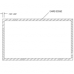
To meet UL requirements, absolute minimum card-edge design clearance for any conductor will be 0.060 inches. This must include any possible tolerance of routing or shearing the board from a panel. From an assembly aspect a minimum edge clearance of 0.150-.200 inches is required on the primary and secondary sides of the PCB.

Internal tracks and planes must not be designed closer than 0.050 inches to the card edge.

3.4 Placement of Polarized Components
It is preferred that all polarized components be placed on the PCB in the same orientation.

3.5 Wave Soldering Layout Guidelines
When discrete components (or active component) require attachment to the secondary side of the PCB utilizing the wave soldering process, special layout rules apply:

  1. Layout components with their termination oriented as shown in Figure 11.
  2. Layout components with acceptable component-to-component clearances as shown in Figure 5. Proper clearances will insure the components will solder proper during wave soldering.
  3. Avoid staggering components as shown in Figure 12A and 12B. Staggering causes a shadowing which results in openings and acceptable distances between components are shown in Figures 12A and 12B.
  4. Do not put bare traces (traces that are not covered wit solder mask) nearer than 0.030 inches to SMT pads on the secondary side. If this rule is violated shorting (bridging) during wave soldering is likely to occur.
  5. The maximum trace width leading to SMT pads can be 0.025 inches. This will eliminate heat sinking effects.
  6. Avoid placing components in heavily heat sinked areas. For example, under large components or connected to a ground plane.

3.6 Via Hole Considerations and Constraints

VIAs used in SMT and FINELINE designs will use 0.015 inch finished diameter holes in a pad with a minimum diameter of 0.032 inches. All vias will be “tented” (covered with solder mask) on both sides of PWB to minimize soldering problems and to insure a good vacuum seal on the incircuit tester.

VIAS that have been tented can be placed under components.

In situations where the VIAS are not tented with solder mask “DO NOT PLACE VIAS UNDER LOW PROFILE COMPONENTS.” Low profile components are defined as components wit bodies less than 0.012 inches above the cards surface. Most discrete resistors and capacitors fall into the low profile category.

Through VIAS are the preferred type but blind VIAS or buried VIAS can be used if required due to space constraints. Blind and buried VIAS should be avoided if possible!

Un-tented VIAS must be a minimum of 0.020 inches from SMT pads (see Figure 7B). If the VIAS are tented, the VIAS must be a minimum of 0.010 inches from respective SMT pads.

3.7 Tooling Hole Requirements
Tooling holes are required for auto assembly processes. The standard tooling hole diameter is 0.127+0.002/-0.000 inches diameter. PWBs will typically be assembled in standard panel form as shown in Figure 9.
All assembly tooling holes must be unplated.

  1. Unplated tooling holes shall be placed on each individual PCB in diagonal corners
  2. The standard tooling hole diameter is 0.127 inches (shall not be less than 0.090 inches in diameter).
  3. Traces must not be closer than 0.050 inches from the tooling holes on the primary and secondary sides of the PCB. Traces must not be closer than 0.025 inches from the tooling holes on inner layers. Components can be no closer than 0.125 inches from the tooling holes.

3.8 Fiducial Mark Requirements

Fiducial marks are required for automatic placement of surface mounted devices (SMDs). The fiducial marks allow the placement equipment to optically recognize the artwork pattern on the PCB. The fiducial marks dimensional requirements are shown in Figure 13.

The fiducial marks should be located in three corners of individual PCBs as shown in Figure 14. Two fiducial marks should also be located around large SMT devices (larger than 68 pin) or fine pitch devices.

3.9 Design for Thermal Balance

If densely populated areas and nondensely populated areas exist on a single layout then thermal mismatch can be experienced during the reflow process. This means components on one area of the card may get too hot while the other areas have cold solder joints.

PLCCs normally cause thermal mismatch due to their size. The following rules apply:

  1. If PLCCs in 9 square inches on the boards result in more than 5 times the mass in any other 9 square inches on the board then, the PLCCs in that area should be a minimum of 0.350 inches apart.
  2. Distribute the surface area of ground planes as uniformly as possible.
  3. Avoid large voids in power and ground planes to minimize warp and signal noise.
  4. Power and ground planes should be on symmetrical layers to minimize warp. They must also be equal distance from the center.
  5. A SMT pad must not be part of ground plane. SMT pads must be a minimum of 0.030 inches from a mass of ground plane.

3.10 Dead Space

Dead space is required for manufacturing since the conveyors are used to transport the boards by its edges during manufacturing processes and for fitting test fixtures. Figure 15 shows dead space requirements.

Alternatives to dead space on individual PCBs are the use of panels or breakouts. Breakaways can be used to handle the board through manufacturing and can be removed after test.

3.11 Components Under Components
Placement of low profile components under other components on the same side of the PCB should be avoided. Components under components are very difficult to inspect, troubleshoot or repair.

3.12 Standard Hole Sizes
Use the minimum number of hole sizes as possible (8 or less).

3.13 Trace Run Paths
Take the shortest practicle distance between two points. Keep traces as far away from exposed conductors as possible. If solder mask is poorly registered or the mask is damaged shorting could occur if circuits are too dense. See Figure 3.

  1. Testability Guideline of SMT layouts

The following guidelines are presented to summarize testability layout rules for PCBs that will utilize an in-circuit test.

  1. Test Pads
  1. A 0.032 inch solid square test pad should be used.
  2. Provide a minimum of one test pad for each specified electrical node, if not accessible at a plated through hole pin.
  3. Test pads should be laid out 0.100 inch centers (0.050 inch is acceptable as a last resort and must be approved by the Test Design Engineering).
  4. Assure all test points are to be laid out on the solder side unless otherwise specified by test design engineering.
  5. No more than 40 test pads are allowed per square inch.
  6. All test pads must be coated with solder to allow good electrical contact during probing. DO NOT APPLY SOLDER MASK ON TEST PADS.
  7. For each voltage and ground, provide at least one test pad for each ½ amp of current (worst case) required to power-up the PCB. A minimum of two test pads for each voltage and ground is required. (Information supplied by Test Design Engineering.)
  8. Test pads should be indicated on final, PPR and DEM schematics.
  9. Test pads will be represented as intelligent parts in the PBA Design and Schematic Capture Tools.
  1. Others
  1. Use pull up or pull down resistors on input lines.
  2. Connect unused gates and control lines to VCC or ground through a resistor.
  3. Interrupt jumpers to isolate sensitive test areas and oscillators.
  4. Probe contact on unused control lines and gate output.
  5. Probe contact on both sides at unused inverters.
  1. PCB MARKINGS
  1. All PWBs using SMT components will require the following markings. Text height shall be a minimum of 0.050 inches.
  1. The company name (minimum 0.100 inches)
  2. Part number (minimum 0.080 inches)
  3. Revision number (minimum 0.080 inches)
  4. Reference designators (minimum .050 inches)
  5. The board drilling number etches in copper on the solder side of the PCB.

If the PBA requires markings to be used by the customer (option blocks, switches, LEDs, etc.) these markings must be screened or etched on the board. A minimum of 0.060 inch text.

A minimum of 0.020 inches designed clearance is required between SMT pads and silkscreened markings.

Ink used must not deteriorate or bleed contaminants on to SMT or thru-hole pads under exposure to IR Reflow, Vapor phase Reflow, Freon cleaning or wave soldering.

  1. DOCUMENTATION REQUIREMENTS

PBA Requirements – Electronic Format
Documentation
Gerber Files – 274X Format
Drill or Fabrication Drawing
Schematic
X-Y Drill Plan
Assembly
Primary Side Assembly Drawing
Secondary Side Assembly Drawing
Silkscreen Drawing
Bill of Materials
SMT Primary Side
SMT Secondary Side
Board Drilling
Board Blank
Drill Plan
Specifications and Layer Configuration Data
Supplemental Mechanical Detail Drawing
Paste Screen
Primary Side Detail
Secondary Side Detail (If required)
Miscellaneous
Test, Performance, and Technical Specs
Mechanical Details (Front Panels, Covers, etc.)
Process Specs

Manufacturing Data
Test
Test Drill Files
Manufacturing
X-Y Coordinates of all Components
Electronic BOM (Excel, CSV, or TXT)
Conventional Component Auto-insertion
Auto Inspection Data
Test Node Data

  1. LIBRARY PAD GEOMETRIES

SMT device shape dimensions will be based on IPC-SM-782. The pad geometries defined must be incorporated into the CAD shape libraries.

When the geometries are updated to improve manufacturability, the CAD date base must be updated. When old designs are updated, the updated pad geometries should be incorporated. ENs and ECOs must specify which pad geometries should change.

  1. DESIGN GUIDELINES CHANGE PROCEDURE

If any new information becomes available or if new requirements arise based on experience the following procedure should be followed to insure the information is documented in the official SMT design guidelines.

  1. Submit the attached “DESIGN GUIDELINES REVISION REQUEST FORM” to the AME manager. Along with the revision request form attach a summary of the proposed change or addition.
  2. The AME group will review the request and call a Design guideline review meeting. The proposed change will be discussed and if approved the proper sign offs will be obtained (see Revision Request Form).
  3. The Design Guidelines will be updated during the first week of each quarter. Revisions will be issued as temporary guidelines until incorporated into the official guidelines.
  4. The attached “Revision Log” must be filled out to reflect each revision.

Figure 4A

Primary Side Layout
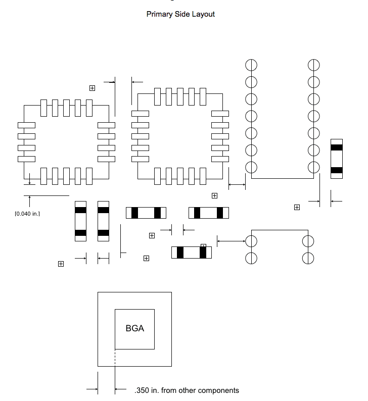
Figure 4B

Primary Side Layout
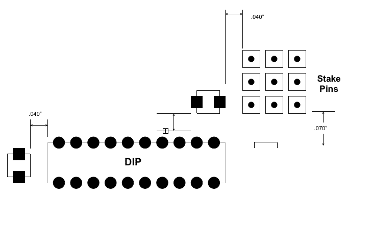
Figure 5

Secondary Side Layout
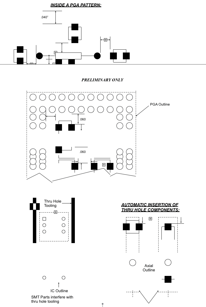
Note: All dimensions in mils/.001 inches (shown from pad to pad)

FIGURE 5 (continued)

Secondary Side Layout
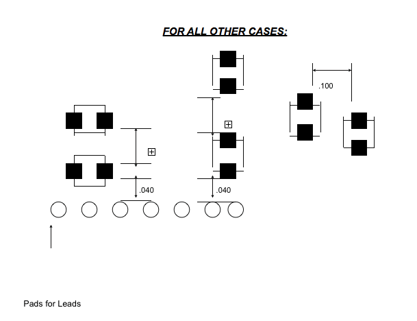
FOR ALL OTHER CASES:

Note: All dimensions in mils/.001 inches (shown from pad to pad)

Figure 6

Clinch Tooling to SMT Clearance (Bottom side)
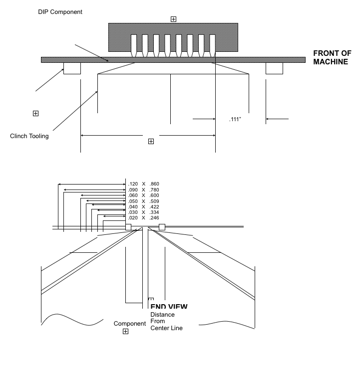
Figure 7A

Acceptable Layout
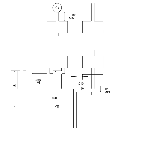
Figure 7B

Acceptable Layout
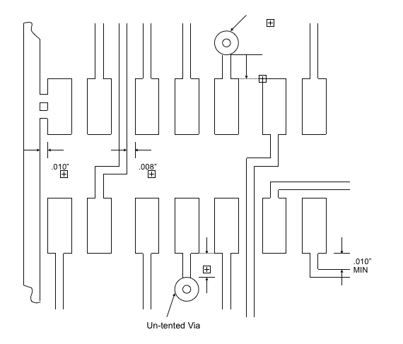
Figure 8A

Unacceptable Layout
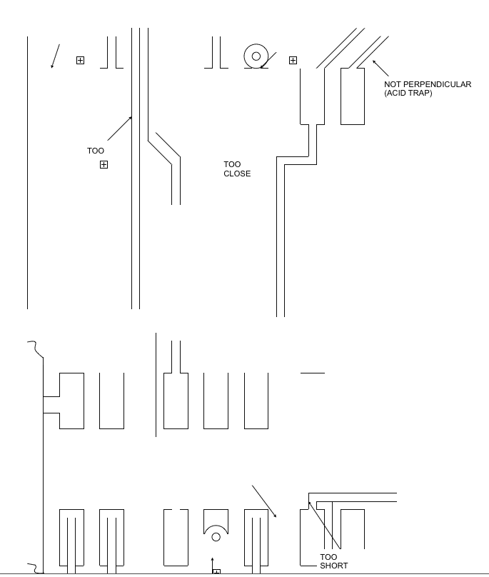
Figure 8B

Unacceptable Layout
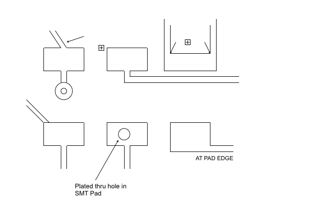
Figure 9
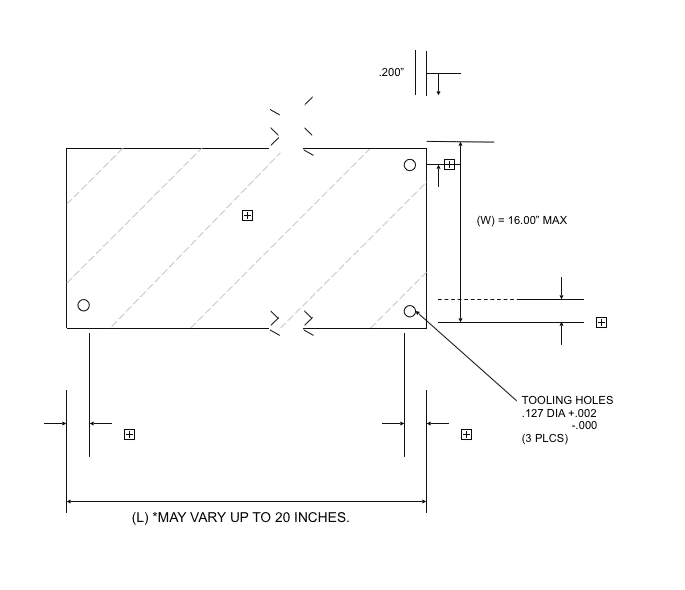
Figure 10A

Figure 10B

Figure 11

Secondary Side Layout
(AVOID IF POSSIBLE)
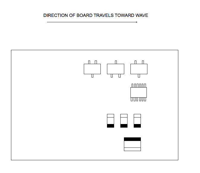
Figure 12A

Avoid staggering wave soldered adjacent chip components
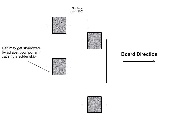
Figure 12B

Secondary Side Layout
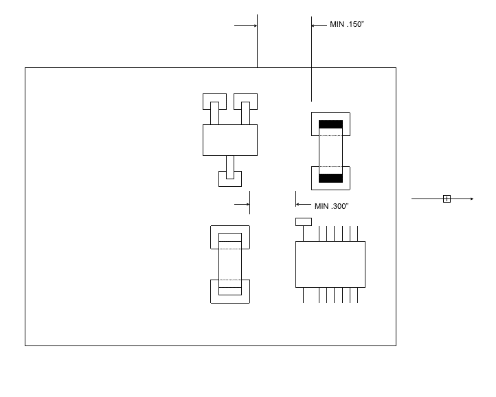
** Avoid staggering or placement of uncommon package types behind each other for wave soldering.

** For mix technology designs, the use of sots, tantalum capacitors, and SOIC’s should be avoided on the secondary side.

Figure 13

Fiducial Pad

Figure 14
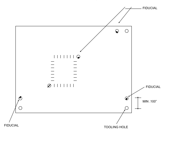
Figure 15

Universal track feeder 45711101 for tube component

Track Feeder supports and positions component tubes for transport to the machine pick position. The track feeder is comprised of a track assembly and the feeder base assembly。
Procedures and Adjustments
The following subsections contain the setup and maintenance procedures that are required for proper track feeder operation. Note that track assemblies are available both with and without an attachment called an isolator. The isolator relieves the level of pressure placed on components, making pick-up by the GSM machine easier. Attaching a Track Assembly With an Isolator Feeder Base Assembly Cover Pneumatic Ports Track Mount Dowel Pins Interface Assembly Track Assembly Isolator Attach a track assembly with an isolator to a track feeder using this procedure. This procedure assumes that you’ve been using a track assembly that does not have an isolator, and that this track assembly is still attached to the track feeder base assembly. If you’re merely replacing one track assembly that has an isolator with a similar track assembly, execute Step 1 of this procedure, omit Steps 2 through 4, and continue with Step 5.

1. Loosen the screws holding the track assembly to the track feeder base assembly, and remove the track assembly.
2. Remove the screws from the feeder cover, and remove the cover from the base machining.

3. Place the interface assembly on top of the track feeder base assembly, centering the interface assembly over the track mount.

4. Connect the two interface assembly air hoses to the valve assembly coupler’s pneumatic ports.

5. Place the new track assembly over the interface assembly and onto the track feeder base assembly. In doing so, position the track assembly so that it fits over the track mount dowel pins.

6. Now, position the interface assembly so that it fits snugly against the track assembly, paying particular attention to achieve a good fit at the end of the track assembly where the isolator is located.

7. Screw the new track assembly to the track feeder base assembly. Torque the screws to 5 inch-pounds.

8. Place the feeder cover back onto the base machining, and screw it securely into place.

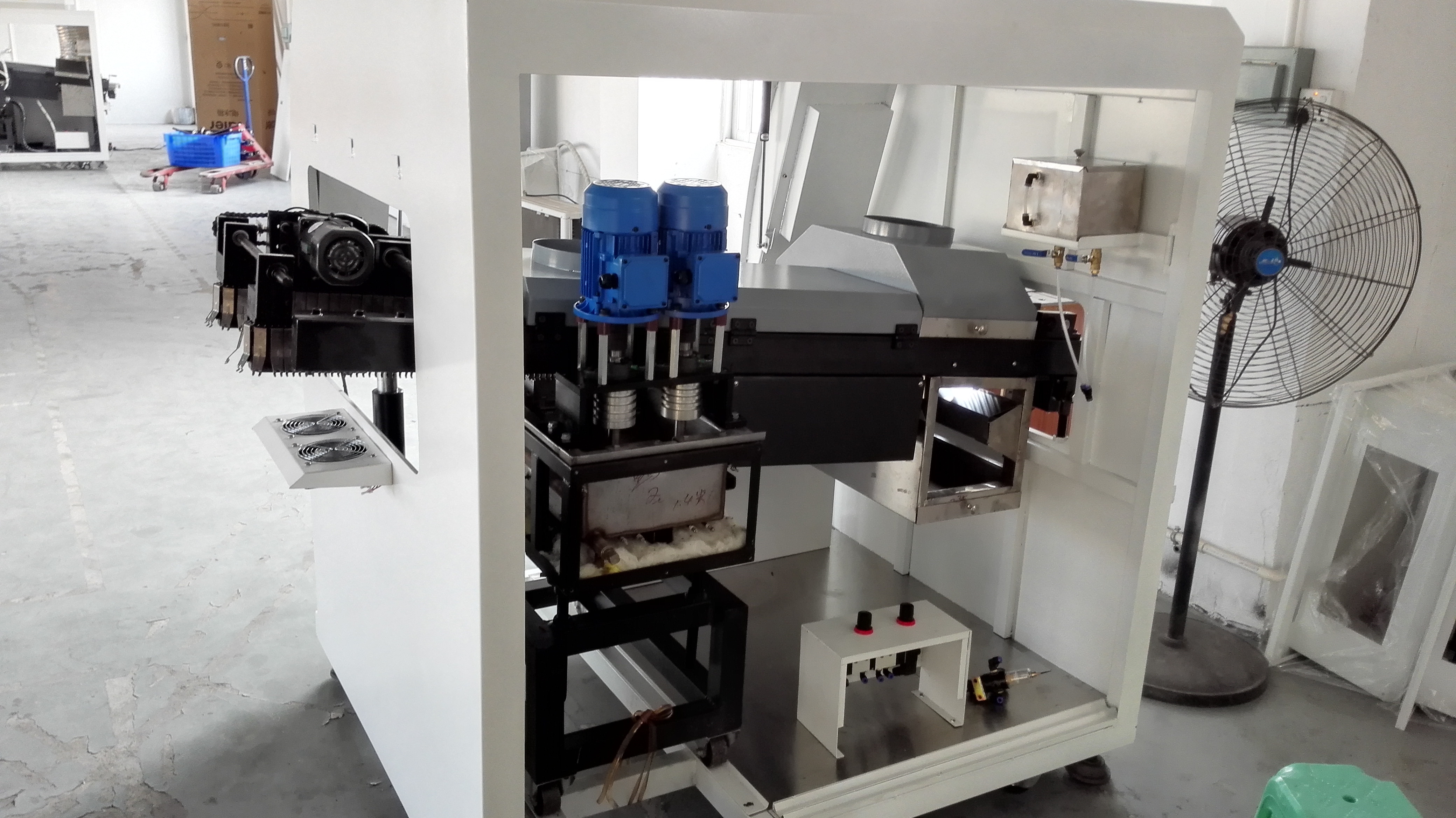
S-7000 Odd Form Component-Automatic Terminal Insertion Machine

1.Operating system: Windows environment to run the operation of the software, the production data, management data , equipment parameters, all I/O signal diagnosis, etc. can be finished on the host with a touch screen.

2.Insertion speed: 0.35 seconds/piece (theoretical), adopts panasonic AC servo drive, high speed, low noise, stable movement.

3.Visual system: Industrial specialized high definition camera and the development of automatic visual correction software of vision system, automatic correction, insertion accurately.

4.Missing part system: when insert the missing part, which can realize a leakage detection and set fill interpolation function, improve the machine availability.

PCBA Quality Process Audit — SMT Pick and Place machine

1. Work Instructions
1.1 Is there a revision controlled Operator Work Instruction which contains loading information for the specific product being built? (Score 0 if any unsigned/undated handwritten instructions or any handwritten instructions more than 48 hrs old)
1.2 Are Work Instructions readily available to the operator and are they followed at Component Placement?
1.3 Are component part numbers and descriptions included on the Work Instructions?
1.4 Are component descriptions sufficiently detailed to check at first-article that the correct components are being used?
1.5 Is the machine head/slot number for component loading specified for each part number on Work Instructions?
1.6 Are the reference designators and the quantity per part number specified on Work Instructions?
1.7 Is the component feeder type/size specified on Work Instructions or otherwise for each component package type?
1.8 Is the machine Program Name specified on the Work Instruction or line set-up instructions?
2. Component Loading and Verification
2.1 Is there an automated bar coded component loading verification aid in order to reduce the probability of incorrect loading? Note*
2.2 Are the component loading verification aids hard linked to the placement program so that loading is verified against program data?
2.3 Can traceability of component lot codes be demonstrated for critical devices?
2.4 Is component loading/changes verified and cross checked by an individual other than the set-up operator at product changeover? Note*
2.5 Is a component loading/changes verification log signed by the set-up operator and countersigned by the cross checker before start up? Note*
2.6 Is the correct feeder loading base used to facilitate real to feeder loading?
2.7 Are first-built boards verified against documentation for missing/misplaced components and for correct component polarity?
2.8 Are first-articles conducted using AOI methods and complemented with description verification and value metering?
2.9 Are all Resistors & Capacitors measured for a value within the tolerance (one per part number) at first-article & at reel change?
2.10 Is a first-article log signed to verify acceptance before start up?
2.11 Is the orientation of Tantalum SMT capacitors, Diodes, etc in tape format, standardized and documented for polarity orientation?
2.12 Is the IC tray loading polarity standardized for each type of polarity indicator that can be used for each component?
2.13 Is loading polarity referenced both from the tray and the component so as to ensure retrayed components are correctly loaded?
3. Nozzles, Feeders, and Tooling
3.1 Is there a document which details the standardized nozzle diameter set-up selected for each type of placement equipment?
3.2 Are these standardized nozzle diameter set-up documents readily available for when nozzles need to be replaced or changed?
3.3 Is there a document which details the range of component XYZ body sizes that each selected nozzle type can successfully place?
3.4 Is there a documented requirement to conduct daily nozzle centering and is there evidence that this is done?
3.5 Is each feeder identified with its own unique serial number?
3.6 Is there a documented and effective Feeder Maintenance Program? Records (s/w or otherwise) must be by Feeder Serial Number.
3.7 Are database records maintained for each feeder serial number for the purpose of tracking its maintenance history and performance?
3.8 Is feeder maintenance history used to monitor feeder life so that problematic feeders can be removed from the process?
3.9 Can it be demonstrated that the number of feeder indexes is counted & monitored for each unique feeder using software or otherwise?
3.10 Is this information used to flag that feeder preventative maintenance is required after x number of indexes?
3.11 Is there a documented requirement to indicate that Blocks or Support Pins are needed for specific products?
3.12 Is the No, location, type and height of Support Blocks/Pins identified on a product by product basis? Score NA if in 3.11 there are not needed.
3.13 Are the Support Pin locations identified for each product using templates/tooling or some other effective solution? Comment as above.
4. Moisture Sensitive Devices
4.1 Are components stored before loading and after unloading in a manner which prevents damage?
4.2 Are the Moisture Sensitive Devices (MSDs) and their sensitivity level readily known to the operator?
4.3 Are MSDs time stamped at opening and their exposure time monitored against pre determined limits?
4.4 Is there a flag to indicate that the exposure time has been exceed for any given device in a dry box?
4.5 Is there a flag to indicate the MSD exposure has expired for any MSD device currently loaded in the placement machines?
4.6 Have MSD procedures been updated to reflect the JEDEC standard for MSD control? (J-STD-033A MSD released in July 2002)
4.7 Is there evidence of correct implementation of J-STD-0033A for all MSD devices?
4.8 Are there MSD procedures in place to ensure MSD shelf life is reduced based on measured Relative Humidity conditions?
4.9 Is there a method in place to address the time spent in dry storage and its effect on remaining life based on MS Level and RH Level?
4.10 Is it clearly understood that MSD ‘shelf life’ continues to degrade during dry cabinet storage of some MSD devices?
4.11 If MSDs are on both sides of a PCBA, is there an effective method to account for time between 1st and 2nd reflow?
4.12 Can MSD control be demonstrated for MSD devices that need internal/external pre-programming?
4.13 Can MSD control be demonstrated for rejected devices and devices used for rework?
4.14 Have MSD recovery methods been defined and adequate for all component types?
4.15 Does the control of Moisture Sensitive Components include those components on reels?

4.16 Is the baking or hot room storage time and temperature documented and controlled for component recovery?
4.17 Has this time and temp been determined based on the component supplier’s guidelines / J-STD-0033A?
4.18 Is there evidence to demonstrate that the control process for MSDs is in use and is effective?
5. Machine Capability
5.1 Are Component Placement Programs generated from CAD XY coordinate data?
5.2 Is there a standardized nomenclature for Shape Code definition?
5.3 Can this nomenclature be used to determine the most appropriate shape code to allocate to a given part of given dimensions?
5.4 Are localized fiducials used for fine pitch devices when localized component fiducials exist on the board?
5.5 Has manual component moving been eliminated given correct CAD, nozzle set-up, Shape Code allocation, local fiducials, Cam speed, etc?

5.6 Does the Fine Pitch placement machine have the capability to check lead Coplanarity in xyz?
5.7 Does the Fine Pitch placement machine use its coplanarity capability on all leads of 20 mil pitch or less, and all programmed parts?
5.8 Does the Fine Pitch placement machine have the capability to check ball arrays? If no such device, score NA.
5.9 Does the Fine Pitch placement machine use its ball array verification capability for all BGA devices? If no such device, score NA.
5.10 Is the machine Program Name revision controlled to show traceability of program changes?
5.11 Is the machine Program Name traceable to the PWB and PCBA part number?
6. PCBA
6.1 Are outputted boards at least sample inspected pre reflow for placement positional accuracy for machine control purposes?
6.2 Is the frequency for this verification defined and documented, and is there evidence to suggest it is followed?
6.3 Is there a visual aid available which identifies the populated locations with polarity, and also the no-pop locations?
6.4 Is there a placement standard pre reflow to validate placement accuracy for the shape code, nozzle allocation, etc. parameters used?
6.5 Is there evidence to demonstrate that action is taken to adjust the machines performance for when this standard is exceeded?
7. Attrition Rates and Rejected Components
7.1 Is attrition rate monitoring conducted systematically to ensure feeder and/or nozzle problems are captured at least hourly?
7.2 Is there documented evidence to ensure attrition rates are checked and actioned at least hourly to ensure process control?
7.3 Is there a specification defined for acceptable attrition rates for the individual feeders?
7.4 Is there a specification defined for the maximum allowable number of nozzle skips per machine before it is shut down for repair?
7.5 Are these specifications determined based on a percentage combined with the number of placements for a given time period?
7.6 Is there evidence to demonstrate that attrition rate monitoring is conducted, effective, and used to make process control decisions?
7.7 Is there a documented process for the disposition or reuse of machine rejected components? Rs and Cs must not be reused even for rework.
7.8 Are rejected components reviewed and repaired to ensure conformance before reuse, even if only used for rework?
7.9 Are there repair blocks available or a lead conditioner in use for repairing ‘real’ Coplanarity rejects? Score 0 if parts not repaired.
7.10 Does the re-traying process always ensure that component polarity wrt the tray and the component loading polarity is preserved?
7.11 Is there a documented Process Deviation procedure to manage machine skips for hand placement if hand placement is allowed?
8. Process Capability
8.1 Has a Process Capability Analyses (PCA) been conducted and the Cpk acceptable for the suite of shape codes in use?
8.2 Were shape code allocations, component nozzle allocations, cam speeds, etc. recorded for this PCA?
8.3 Are the recorded shape code allocations, component nozzle allocations, and cam speeds, the same as those used today?

PCBA Quality Process Audit — Wave soldering machine

1. Work Instructions
1.1 Is there a revision controlled Operator Work Instruction which contains set-up information for the specific product being processed? (Score 0 if any unsigned/undated handwritten instructions or any handwritten instructions more than 48 hrs old)
1.2 Are Work Instructions readily available to the operator and are they followed at Wave?
1.3 Do Set-Up Sheets specify the Solder, the Flux, and the thinners (as applicable) to be used?
1.4 Do Set-Up Sheets specify the Spray Flux parameter settings such as delay, duration, traverse speed, pressure, etc?
1.5 Do Set-Up Sheets specify the Pre-Heater set points and the Solder Pot Temperature and are they the same as those on the machine?
1.6 Do Set-Up Sheets specify the Conveyor Speed and is it the same as that in the program?
1.7 Do Set-Up Sheets specify the Lead Clearance and is it the same as that set by the machine?
1.8 Do Set-Up Sheets specify Wave Type (Chip/Lambda/Omega) to be used?
1.9 Do Set-Up sheets specify the Solder Pot Hot Air Knife Pressure and Temperature settings?
1.10 Do Set-Up sheets specify if the Finger Cleaner must be on? No Finger Cleaner = 0
1.11 Is the machine Program Name specified on the Work Instruction or set-up sheets?
1.12 Do the all the above wave parameter settings correspond to those settings on the machine?
1.13 Are Generic Wave Set-Up Parameters documented? These are the parameters which are not changed for product changeovers.
1.14 Do these Generic Wave Set-Up Parameters include, pressure settings, conveyor angle, etc.
2. Machine Capability
2.1 Is the flux application technology in use suitable for the product being built?
2.2 Is the wave technology in use suitable for the product being built in terms of the ability control critical parameters to achieve desired results?
2.3 Does the wave use a top side pre-heater to ensure PTH barrel fill meets IPC 610 specs given the mass of the board, carrier, and the top hat?
2.4 Are air flow controllers or a centralized control system used to balance exhaust flow rates for each individual exhaust drops?
2.5 Are exhaust flow rate ranges specified and monitored on a regular basis to insure compliance?
2.6 Is Automatic Wave Height control installed to control the laminar wave height?
2.7 Is there a Solder Pot Hot Air Knife installed and used on the wave equipment?
2.8 Is there an automatic Finger Cleaner installed and used on the wave equipment with an appropriated cleaning fluid? No FC = 0
2.9 Is the machine Program Name revision controlled to show traceability of program changes?
2.10 Is the machine Program Name traceable to the PCB and PCBA part number?
2.11 Is access to the machine program password protected with restricted access?
2.12 Do program changes to critical parameters during machine control remain unsaved unless approved by a technician/engineer?
2.13 Is the safety equipment and protective clothing provided adequate and are they used? Must include boots, apron, gloves, face shield, etc
3. Flux Application
3.1 Is flux applied using either a fixed nozzle or moving nozzle spray application method? Any other application method = 0
3.2 Can the sequence of; detection, delay, trigger, duration, and stop, be clearly explained by a technician? Other method = 0
3.3 Is the detection, delay, trigger, duration, and stop, controls performing as expected? Other method = 0
3.4 Is there a feedback link between the conveyor speed and the flux applicator to auto-compensate for changes? Other method = 0
3.5 Is there an automatic sensor that indicates when a flux drum is near empty?
3.6 Is there a method to determine if the quantity of flux applied to the board to ensure it adequate? Not too much and not too little.
3.7 Is there a test used to check the coverage of flux applied to the board to ensure it is sufficient?
4. Wave Set-Up
4.1 Has specifying the Solder Pump Speed value been discontinued as a way to achieve the desired Wave Height?
4.2 Is the relationship between Wave Height set-up and Contact Area/Length known for the product being processed?
4.3 Is there a Quartz Plate available to verify Contact Area/Length achieved for the board being processed?
4.4 Is the documented Contact Area/Length being achieved for the Wave Height set-up used?
4.5 Does the shape of the Contact Area indicate parallelism?
4.6 Does the Contact Length coupled with the Conveyor Speed, achieve the documented dwell time requirement?
4.7 Is there evidence that Contact Area/Length and shape verified after Solder Pot removal and replacement, and maintenance?
4.8 Is there evidence that the Contact Area/Length and shape verified on addition of solder or on adjustment of lead clearance?
4.9 Does the board/pallet exit the Solder Pot in the stagnant area for the set conveyor angle and lead clearance?
4.10 Are all conveyor Fingers in a good state of repair?
4.11 Is the quantity, type and spacing of each Finger design defined for the conveyor?
4.12 Has the pot been set up to run with an intermittent wave so as to reduce dross build up? If gap between subsequent PCBAs too small, score 1
4.13 Does the level of Dross in the pot suggest that the pot is dedrossed at least once every 8 hours?
5. Temperature Profile
5.1 Is there available a Temperature Profile for the product currently being built?
5.2 Is the Temperature Profile assessable and readily available to operators / technicians as and when required?
5.3 Were the Pre-Heat Set Points, Conveyor Speed, and Solder Temperature logged for that Thermal Profile when it was conducted?
5.4 Do the Set Points, Conveyor Speed & Solder Temp written on the Thermal Profile correspond to the current Machine settings?
5.5 Is there available an Engineering based specification to detail the acceptable process window for Temperature Profiles?
5.6 Was the Engineering based spec. derived from the Flux manufacturer’s recommendations but controls to a narrower window?
5.7 Does the product Temperature Profile fall within the Engineering based specification for the process window?
5.8 Does the product Temperature Profile fall within the Engineering based specification for glass transition temperature requirements?
5.9 Can any excursions outside of the process window be justified and supported with hard evidence and logical analysis?
5.10 Does the product Temperature Profile meet the requirements of the SMT components already attached to the PCBA?
5.11 Are the boards used to establish the initial Thermal Profile kept as engineering samples?
5.12 Have at least five thermocouples been used at various points on the board to establish the Thermal Profile? Note*
5.13 Is there a documented and systematic approach used to identify the most appropriate locations to attach the thermocouples?
5.14 Is there evidence that each thermocouple ball was bonded to a board joint using Hi Temp. Solder or Conductive Epoxy?
5.15 Is the top side Temperature Profile low enough to prevent secondary reflow? Must be below 160 degrees C.
5.16 Has a Calibration Profile been established in order to detect machine long term performance degradation?
5.17 Is there a documented frequency for running a Calibration Profile and was it established based upon historical performance data?
5.18 Is there evidence to demonstrate that Calibration Profiles are conducted and that records are up-to-date?
5.19 Is the practice of comparing the current Calibration Profile to the Standardized Calibration Profile used to identify changes?
5.20 Is the current Calibration Overlay/Profile used to determine if a variation in the wave’s thermal characteristics has occurred?
5.21 Is the current Calibration Overlay/Profile used to determine if a variation in conveyor speed has occurred?
5.22 Is there evidence to demonstrate that action was taken when the Calibration Profile was different to the Standard?
5.23 Is a standardized tool, like a WaveRider, used with a standardized profile to conduct a Calibration Profile?
6. Solder Analysis
6.1 Is there a documented frequency for conducting Solder Analysis and was this frequency established based upon historical results?
6.2 Is there evidence to demonstrate that Solder Analysis records are up-to-date?
6.3 Does the Solder Analysis results suggest that contaminants in the solder pot are within acceptable levels?
6.4 Is there evidence to demonstrate that action was taken when Solder Analysis results were unsatisfactory?
7. Manual Inspection
7.1 Are outputted boards at least sample inspected post wave for wave solder defects as part of machine performance control?
7.2 Are Workmanship Standards defined for soldering, and are they accessible so that machine performance can be measured accurately?
7.3 Is Defect Density Charting used to identify the common location of defects so that actions may be take to eliminate them? This may include addition of solder thieves, pallet/carrier modification, etc.
7.4 Is there evidence of the use of at least sampling X-ray to ensure via penetration and barrel fill are to acceptable standards?

PCBA Quality Process Audit — Manual Assembly

1. Work Instructions Enter 1 or 0. NA may be a valid response for shaded cells.^
1.1 Are revision controlled Work Instructions displayed for the operator at each assembly station? (Score 0 if any unsigned/undated handwritten instructions or any handwritten instructions more than 48 hrs old)
1.2 Are component part numbers and their descriptions specified on Work Instructions?
1.3 Are component descriptions sufficiently detailed to ensure the correct component is being used?
1.4 Are the reference designators and the quantity per part number specified on Work Instructions?
1.5 Is component polarity or its non-existence consistently and unambiguously specified on Work Instructions?
1.6 Are the components on the Work Instructions listed by the most appropriate order of insertion?
1.7 Is the layout of lin bins/trays defined on Work Instructions for each assembly station?
1.8 Are all lin bins/trays located in the correct position as per Work Instructions for each assembly station?
1.9 Do Work instructions indicate if solder pallets/carriers or breakers must be used?
1.10 Do Work instructions indicate if a top hat, separators, plugs, Kapton tape, finger protection, etc. must be used?
1.11 Does the direction of build for the board align with the orientation of the board on the Work Instructions and Wave direction?
1.12 Do Work Instructions not only indicate what components need to be inserted but also the buddy check components?
1.13 Is the conveyor at entry to the wave, slower than the wave conveyor speed, and documented on Work Instructions?
1.14 Is there a documented process for the identification and control of non-completed boards resulting from breaks, shift changes, etc.
1.15 Is the PWB part number and Revision specified on the Work Instruction or line set-up instructions?
1.16 Does the PWB part number and Revision cross-reference to the PCBA part number and Revision?
2. Station Breakout 1, 2 3, 4 5, 6 7, 8 9, 10 Actual
2.1 Is there a document available which describes the guidelines for station breakout at Manual Assembly?
2.2 Has the number of assembly stations required been determined scientifically in order to maximize throughput within constraints?
2.3 Is there evidence that the line is evenly balanced with the defined number of stations and the defined station breakout?
2.4 Is there evidence to demonstrate that the assembly operators follow the defined station breakout on the Work instructions?
2.5 Is there evidence that sufficient time is allocated for component insertion at each station, as determined by the beat rate of the line?
2.6 Does following the breakout ensure that the insertion of subsequent components is not restrictive or increased in difficulty?
2.7 Does following the breakout ensure that ‘snap-in’ type components are inserted first or off-line?
2.8 Does following the breakout ensure that components that ‘look’ alike are assembled at different and non-adjacent stations where possible?
2.9 Does following the breakout ensure that components that ‘fit’ alike are assembled at different and non-adjacent stations, where possible?
3. Line Set-Up and Verification 1, 2 3, 4 5, 6 7, 8 9, 10 Actual
3.1 Are all Manual Assembly station set-ups verified according to Work Instructions and a log signed prior to start-up http://xanaxonlinebuy.com & re-start?
3.2 Are first-built boards verified against documentation for missing components, value, and for correct polarity pre Wave?
3.3 Are the components supplied to Manual Assembly appropriately prepped with correct lead length, forming and pitch, etc.?
3.4 Is it evident that lead snipping has been minimized through adequate component prep and/or pallet support design?
3.5 Are all totes or tray locations identified with printed part numbers, descriptions, circuit designators, station number, and/or layout information?
3.6 Are boards conveyed along the line automatically without the need to manually push the board forward or pull the board back?
4. Tooling 1, 2 3, 4 5, 6 7, 8 9, 10 Actual
4.1 Is tooling used to provide underside support on all sides, to minimize flexing, for the insertion of components that require a force or snap-in fit?
4.2 Is tooling used and is it adequate to prevent board flexing during all component insertion?
4.3 Is tooling used for snap-in components prone to bent pins, to verify the pin straightness prior to their insertion?
4.4 Is there a document available which describes the guidelines for pallet/carrier design?
4.5 Are footprint, co-planarity, depth below datum, ID, clamping mechanisms, chamfering, direction of flow, criteria addressed?
4.6 Are pallets/carriers identified by a name or tooling number which is traceable to the PCBA part number and revision?
4.7 Is pallet/carrier orientation to the line specified or indicated and correct?
4.8 Are pallets/carriers designed such a way that they support all non-snap-in components without the use of weights?
4.9 Are pallets/carriers appropriately milled out to avoid shadowing and insufficients?
4.10 Do selective wavesolder pallets/carriers use built in solder thieves to help reduce the occurrence of solder bridging?
4.11 Is there a documented requirement to clean pallets/carriers and to regularly inspect them for damage and is there evidence of this?
4.12 Are pallets/carriers in a good state of repair, clean, and satisfactorily stored to prevent damage?
5. Manual Inspection 1, 2 3, 4 5, 6 7, 8 9, 10 Actual
5.1 Are outputted boards 100% inspected pre wave (Top Side) for missing components, value and polarity?
5.2 Is there evidence to demonstrate that this quality inspection is conducted?
5.3 Is there a visual aid (hard copy or otherwise) which identifies the populated locations with polarity, and also the no-pop locations?
5.4 Is there a buddy check system used between stations to ensure the previous operation has been fully completed?
5.5 Is there evidence to demonstrate that a buddy check system is deployed between assembly stations?
5.6 Is the touch method used as part of the buddy system?
5.7 Are manually inserted components that are not tested by ICT specifically targeted for inspection in addition to the buddy check?
5.8 Is there evidence to demonstrate that at least an hourly defect feedback process to Manual Assembly is in operation and effective?
5.9 Is accountability for Manual Assembly defects traceable to a specific workstation and operator/supervisor?
5.10 Are snap-in connectors inspected for bent pins post-insertion? (Tooling or an alternate method with proven effectiveness must be used).
Maximum Score 53 53 53 53 53 53
Score Obtained 0 0 0 0 0 0
Score Percentage 0%
Pass Percentage 80% 80% 80% 80% 80% 80%
Outcome Not Audited Not Audited Not Audited Not Audited Not Audited Not Audited

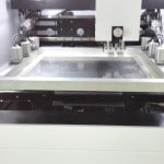
One advanced way to increase your printing accuracy

*Accurate CCD vision positioning and PCB conveying system
*Automatic and effective stencil wiping system,such as dry,wet and vacum cleaning
*Automatic stencil positioning,adjustable size range from 370*470mm to 737*737mm
*Z axis lifting and CCD profile adoption of pulsating CVT mode to guarantee machine’s accuracy
and stable running

AI spare parts、Universal Parts,UIC,TDK.VCD Sequencer.SMT,THT,PCB,PCBA,AI,wave soldering,reflow oven,nozzle,feeder,wave soldering,PCB Assembly, LED, LED lamp, LED display,

SMT Pick And Place machine Spare parts

We can supply smt machine parts, smt spare parts, replacement parts for pick and place machine, Brands including FUJI, SIEMENS, PANASONIC, JUKI, YAMAHA, , etc.


Part of product list: 

Compatible for

Part name

Part No.

Usage

fuji NXT H01

H01 Filter (with plastic BKT)

AA1FZ01

Consumable parts

fuji NXT H12

H12 Filter (with plastic BKT)

AA19H02

Consumable parts

fuji NXT H01

H01 smt filter

XH00560

Consumable parts

fuji

smt pin thick pin

ADCQK8010

replacement parts

fuji

smt pin thin pin

ADCQK8010

replacement parts

fuji XP243

XP243 U axis PULLEY

AGFTR8220

replacement parts

fuji XP243

XP243 U axis PULLEY

AGFTR8230

replacement parts

fuji

fuji sliding block and thimble

O0186

replacement parts

fuji CP6

CP6 HOLDER

AWPH3110

replacement parts

fuji CP43

CP43 CLUTCH

MPH0501

replacement parts

fuji QP242

QP242 Filter

H3022T

Consumable parts

fuji CP41

CP41 press button

O0191

replacement parts

fuji IP3

IP3 Filter

H30215

Consumable parts

fuji CP6

cylinder

WPA5150

Consumable parts

fuji CP7 CP8

smt filter

DCPH3780

Consumable parts


AI spare parts、Universal Parts,UIC,TDK.VCD Sequencer.SMT,THT,PCB,PCBA,AI,wave soldering,reflow oven,nozzle,feeder,wave soldering,PCB Assembly, LED, LED lamp, LED display,
H10212
angela@smthelp.net

AI spare parts、Universal Parts,UIC,TDK.VCD Sequencer.SMT,THT,PCB,PCBA,AI,wave soldering,reflow oven,nozzle,feeder,wave soldering,PCB Assembly, LED, LED lamp, LED display,
H13362
angela@smthelp.net

AI spare parts、Universal Parts,UIC,TDK.VCD Sequencer.SMT,THT,PCB,PCBA,AI,wave soldering,reflow oven,nozzle,feeder,wave soldering,PCB Assembly, LED, LED lamp, LED display,
H30105
angela@smthelp.net

AI spare parts、Universal Parts,UIC,TDK.VCD Sequencer.SMT,THT,PCB,PCBA,AI,wave soldering,reflow oven,nozzle,feeder,wave soldering,PCB Assembly, LED, LED lamp, LED display,
H42693
angela@smthelp.net

AI spare parts、Universal Parts,UIC,TDK.VCD Sequencer.SMT,THT,PCB,PCBA,AI,wave soldering,reflow oven,nozzle,feeder,wave soldering,PCB Assembly, LED, LED lamp, LED display,
K1006L COUPLING
angela@smthelpl.com

AI spare parts、Universal Parts,UIC,TDK.VCD Sequencer.SMT,THT,PCB,PCBA,AI,wave soldering,reflow oven,nozzle,feeder,wave soldering,PCB Assembly, LED, LED lamp, LED display,
H3022T
angela@smthelp.net

AI spare parts、Universal Parts,UIC,TDK.VCD Sequencer.SMT,THT,PCB,PCBA,AI,wave soldering,reflow oven,nozzle,feeder,wave soldering,PCB Assembly, LED, LED lamp, LED display,
H3022L
angela@smthelp.net

AI spare parts、Universal Parts,UIC,TDK.VCD Sequencer.SMT,THT,PCB,PCBA,AI,wave soldering,reflow oven,nozzle,feeder,wave soldering,PCB Assembly, LED, LED lamp, LED display,
H2002Y
angela@smthelp.net

AI spare parts、Universal Parts,UIC,TDK.VCD Sequencer.SMT,THT,PCB,PCBA,AI,wave soldering,reflow oven,nozzle,feeder,wave soldering,PCB Assembly, LED, LED lamp, LED display,
GFPH2540
angela@smthelp.net

AI spare parts、Universal Parts,UIC,TDK.VCD Sequencer.SMT,THT,PCB,PCBA,AI,wave soldering,reflow oven,nozzle,feeder,wave soldering,PCB Assembly, LED, LED lamp, LED display,
GFPN1160
angela@smthelp.net

AI spare parts、Universal Parts,UIC,TDK.VCD Sequencer.SMT,THT,PCB,PCBA,AI,wave soldering,reflow oven,nozzle,feeder,wave soldering,PCB Assembly, LED, LED lamp, LED display,
H1124D
angela@smthelp.net

AI spare parts、Universal Parts,UIC,TDK.VCD Sequencer.SMT,THT,PCB,PCBA,AI,wave soldering,reflow oven,nozzle,feeder,wave soldering,PCB Assembly, LED, LED lamp, LED display,
A10397
angela@smthelp.net

AI spare parts、Universal Parts,UIC,TDK.VCD Sequencer.SMT,THT,PCB,PCBA,AI,wave soldering,reflow oven,nozzle,feeder,wave soldering,PCB Assembly, LED, LED lamp, LED display,
2MGKCF001600
angela@smthelp.net
XS01802=XS03693 SPOOL NXT 原装全新..