Dispenser for high precision products

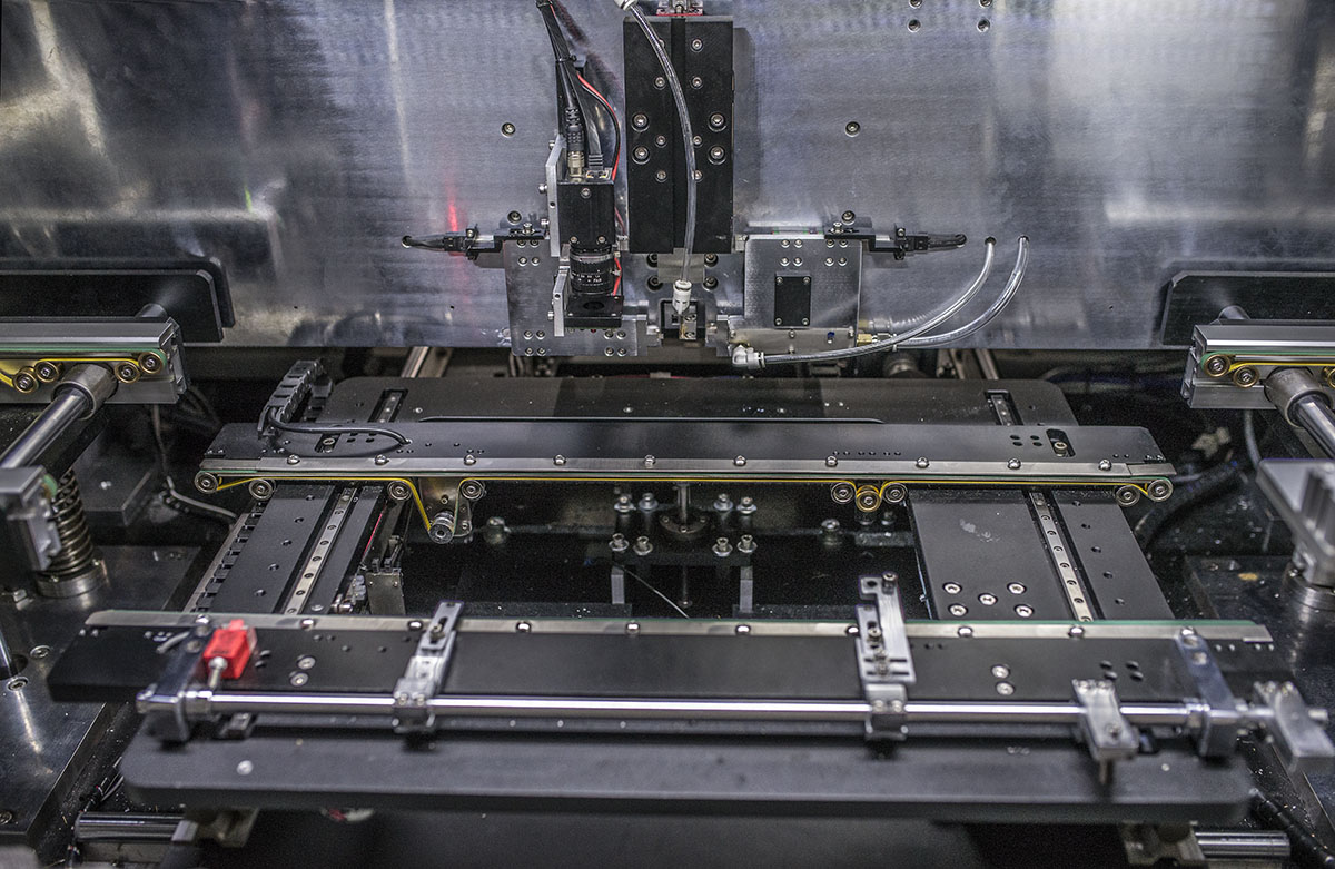
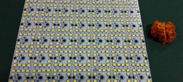
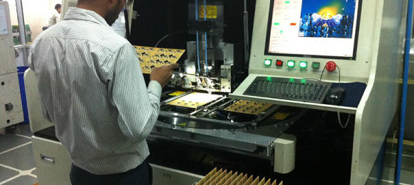
Fully automatic dispensing system bench top automatic visual glue dispenser  Automatic visual glue dispenser    is used to Chevrons,  fridge magnets, key chains,  power supply, cell phone,energy saving light, LED, DVD, DC, Switch, Connector, relay and other industries needing fluid glue solder.

Feature of  Glue dispensing equipment

1 Improve the production efficiency,reduce artifical loss.

2 Equipped with high performance CCD vision positioning system,visual dispensing route,improve accuracy.

3 Use industrial computer to control  operating system,

4 According to the different artifacts, choose suitable LED light source for lighting.

5 Adopt servo motor, ball screw drive.

6 It can arbitrary match with needle valve, diaphragm valve,screw valve, pnematic injection valve, piezoelectric injection valve.


Acceptability for Electronic Assemblies :Soldering Acceptability Requirements

Acceptability for Electronic Assemblies :Soldering Acceptability Requirements


Target-Class1,2,3
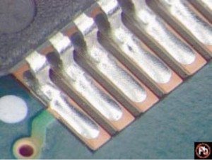
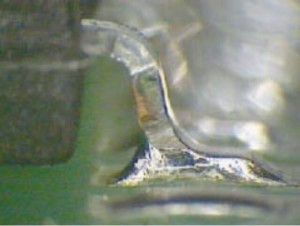
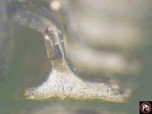
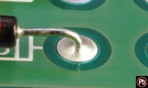
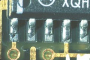
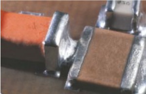
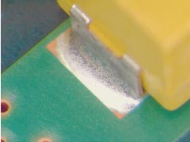
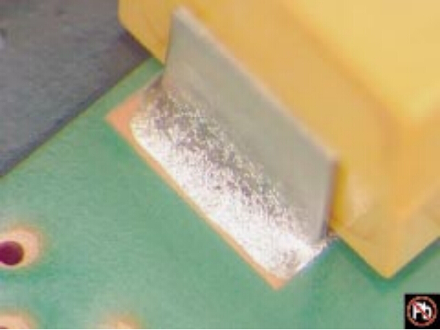
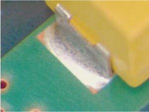
.Solder fillet appears generally smooth and exhibits good wetting of the solder to the parts being joined.
.Outline of the parts is easily determined.
.Solder at the part being joined creates a feathered edge.
.Fillet is concave in shape.


p1s1

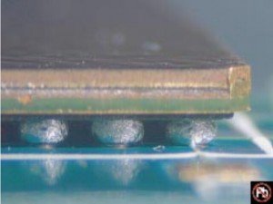
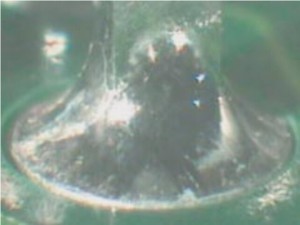
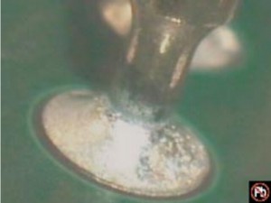
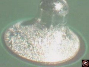
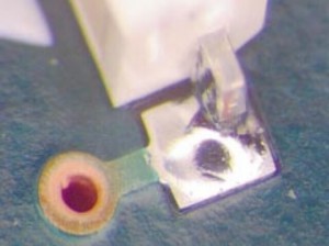
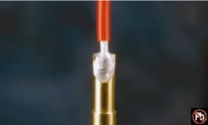
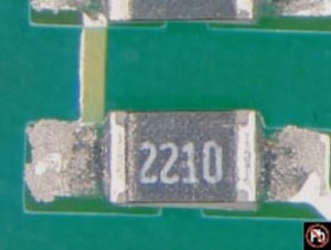
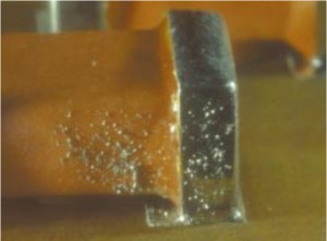
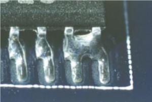
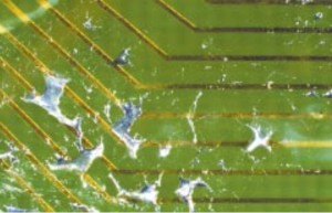
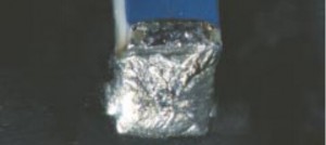
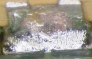
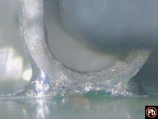
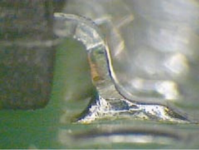
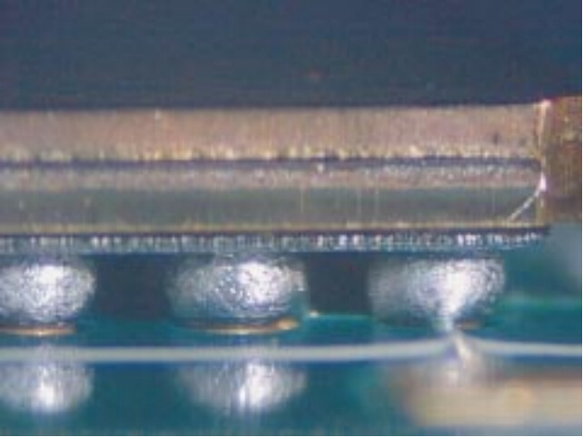
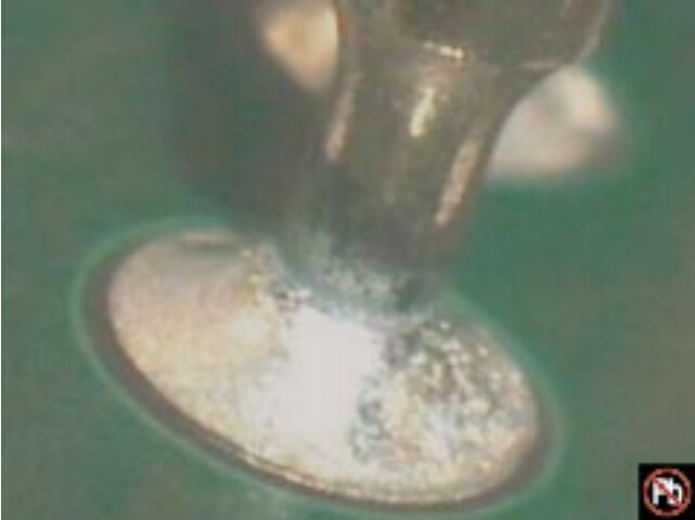
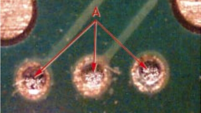
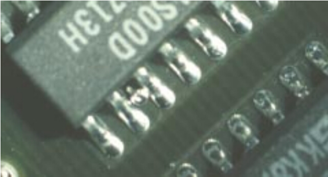
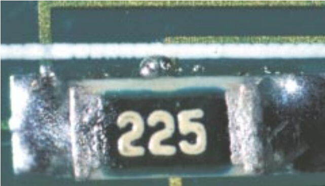
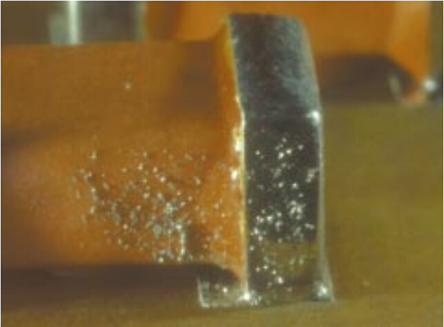
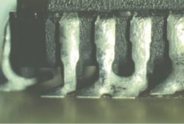
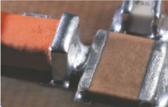
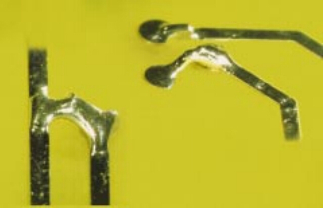
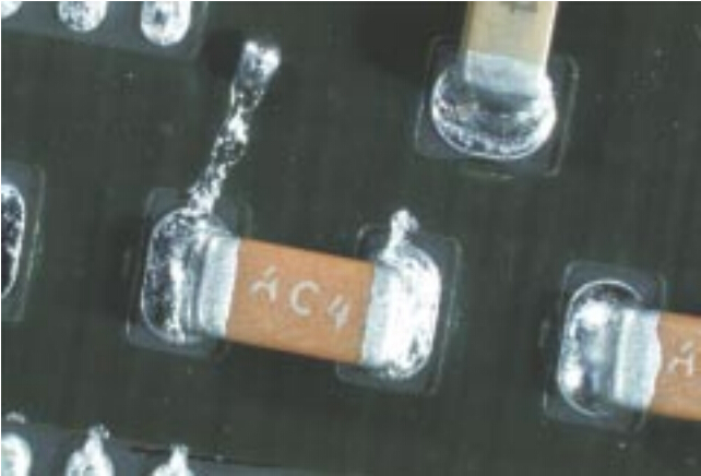
See pic for examples of soldering anomalies.

Acceptable-Class1,2,3
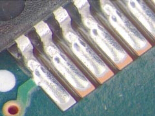
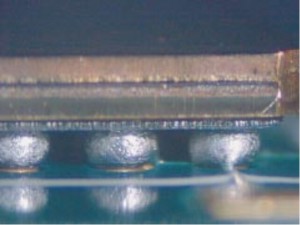
.There are materials and processes,e.g.,lead free alloys and slow cooling with large mass PCBs, that may produce dull
matte,gray,or grainy appearing solders that are normal for the material or process involved.These solder connections
are acceptable.
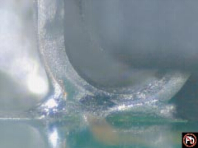
.The solder connection wetting angle (solder to component and solder to PCB termination do not exceed 90°(Figure).
.As an exception,the solder connection to a termination may exhibit a wetting angle exceeding 90°(Figure)when it is 

created by the solder contour extending over the edge of the solder able termination area or solder resist.


p1s2


Figures below illustrate acceptable solder connections with various solder alloys and process conditions.

p2s1 p2s2

SnPb Solder; No Clean Process                                     SnAgCu Solder;No Clean Process
p2s3 p2s4

    SnPb Solder;Water Soluble Flux                                 SnAgCu Solder;Water Soluble Flux

p2s5 p2s6

   SnPb Solder; Water Soluble Flux                                 SnAgCu Solder;Water Soluble Flux

p3s1 p3s2

     SnAgCu Solder;No Clean Process,N2 Reflow                 SnAgCu Solder,No Clean Process;Air Reflow

p3s3 p3s4

      SnPb Solder;No Clean Process                                  SnAgCu Solder;No Clean Process

p3s5 p3s6

     SnPb Solder;No Clean Process                                   SnAgCu Solder;No Clean Process
p4s1 p4s2

                        SnPb Solder                                                      SnAgCu Solder

p4s3 p4s4

                     SnPb Solder                                                           SnAgCu Solder

p4s5 p4s6

         SnPb Solder ; OSP Finish                                                       SnAgCu Solder; OSP Finish

p5s1 p5s2

                     SnAg CuSolder                                                      SnAg CuSolder

p5s3 p5s4

                 SnAgCu  Solder                                                         SnAgCu Solder


       Soldering Anomalies-Exposed Basis Metal

Exposed basis metal on component leads,conductors or land surfaces from nicks,scratches,or other conditions cannot exceed
there quirements of 7.1.2.3 for leads and 10.2.9.1 for conductors and      lands.
Component leads,sides of land patterns,conductors,and use of liquid photo image able solder resist,can have exposed basis
metal per original designs.
Some printed circuit board and conductor finishes have different wetting characteristics and may exhibit solder wetting only to
specific areas. Exposed basis metal or surface finishes should be considered normal under these circumstances,provided the
achieved wetting characteristics of the solder connection areas are acceptable.


Acceptable-Class 1,2,3
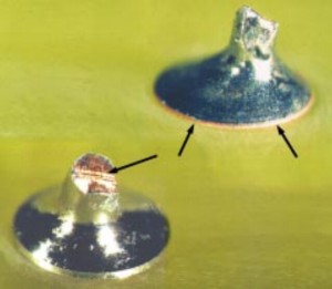
.Exposed basis metal on:
.Vertical conductor edges.
.Cut ends of component leads or wires.
.Organic Solderability Preservative (OSP) coated lands.
.Exposed surface finishes that are not part of the required solder fillet  area.
p6s1 p7s1


Acceptable-Class 1

Process Indicator-Class 2,3

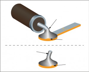
.Exposed basis metal on component leads,conductors or land surfaces from nicks or scratches provided conditions

do not exceed the requirements of7.1.2.3 for leads and 10.2.9.1 for conductors and lands.
p7s2


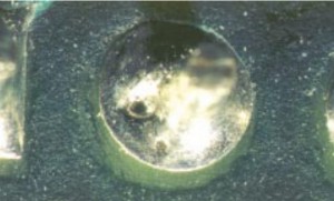
 Soldering Anomalies-Pin Holes/Blow Holes


Acceptable-Class1
ProcessIndicator-Class2,3

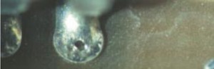
.Blowholes (Figures 1,2),pinholes (Figure 3),voids (Figures 4,5),etc.,providing the solder connection meets all other requirements.


p8s1 p8s2                           

                          1                                                                                2                                                                        

p8s3 p8s4

                             3                                                                                 4

 p8s5                     

                                  5

Defect-Class 2,3

Solder connections where pin holes,blowholes,voids,etc.
reduce the connections below minimum requirements(not shown).


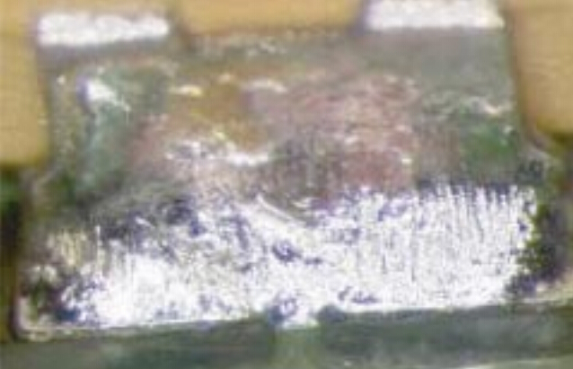
Soldering Anomalies-Reflow of Solder Paste

 Defect-Class1,2,3
.Incomplete reflow of solder paste.


p9s1

 p9s2


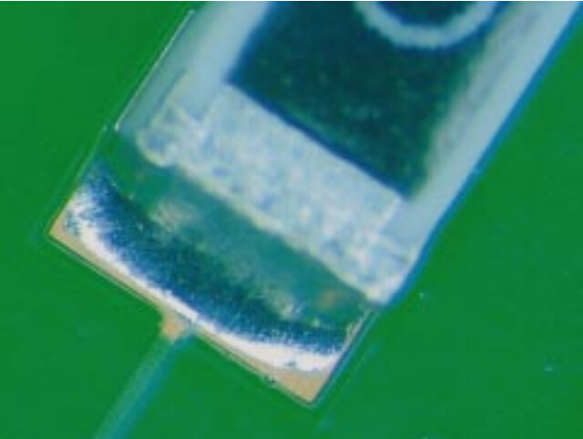
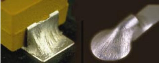
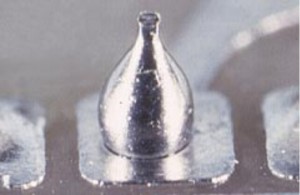
Soldering Anomalies-Nonwetting

IPC-T-50 defines nonwetting as the inability of molten solder to form a metallic bond with the basis metal.In this Standard,that
includes surface finishes.

Defect-Class 1,2,3
.Solder has not wetted to the land or termination where solder is required.
.Solder coverage does not meet requirements for this termination type.

p10s1

p10s2

p10s3

p10s4

p10s5


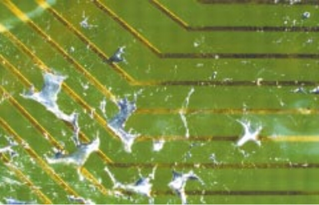
Soldering Anomalies-Dewetting

Defect-Class 1,2,3
.Evidence of dewetting that causes the solder connection to not meet the SMT and thru-hole solder fillet requirements.


p11s1

p11s2

p11s3


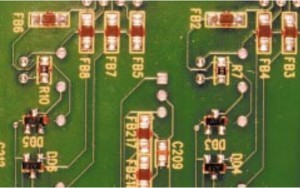
                          Soldering Anomalies-Excess Solder-Solder Balls/Solder Fines

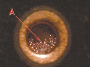
Solder balls are spheres of solder that remain after the soldering process.Solder fines are typically small balls of the original 

solder paste metal screen size that have splattered around the connection during there flow process.


Target-Class 1,2, 3
.No evidence of solder balls on the printed wiring assembly.
p12s1

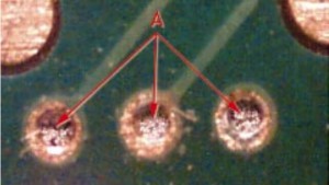
Acceptable-Class 1,2,3
.Solder balls are entrapped/encapsulated and do not violate minimum electrical clearance.
 Note:Entrapped/encapsulated/attached is intended to mean that normal service environment of the product will not cause a solder ball to become dislodged.
p12s2


Defect- Class 1,2,3
.Solder balls violate minimum electrical clearance.
.Solder balls are not entrapped in no-clean residue or encapsulated with conformal coating,

or not attached(soldered)to a metal surface.

p13s1

p13s2

p13s3

p13s4


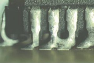
Soldering Anomalies-Excess Solder-Bridging


Defect-Class 1,2,3
.A solder connection across conductors that should not be joined.
.Solder has bridged to adjacent noncommon conductoror component.
p14s1

p14s2

p14s3

p14s4


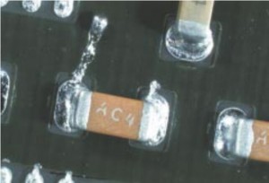
Soldering Anomalies-Excess Solder-Solder Webbing/Splashes

Defect-Class 1,2,3
.Solder splashes/webbing.

p15s1

p15s2


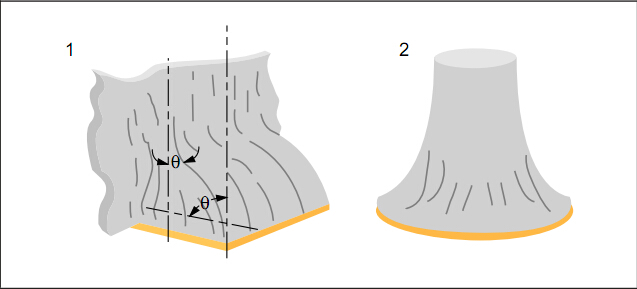
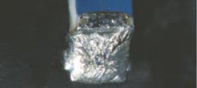
Soldering Anomalies-Disturbed Solder

Surface appearance with cooling lines as shown in Acceptable pic is more likely to occur in lead free alloys and is not a disturbed solder condition.

p16s1


Defect-Class 1,2,3
Characterized by stress lines from movement in the connection (SnPb alloy).

p16s2

p16s3

p16s4

p16s5


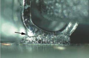
Soldering Anomalies-Fractured Solder


Defect-Class 1,2,3
Fractured or cracked solder.


p17s1

p17s2


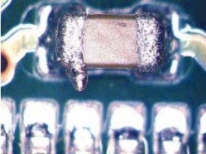
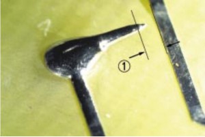
Soldering Anomalies-Solder Projections

Defect-Class 1,2,3
.Solder projection,figure 1,violates assembly maximum
height requirements or lead protrusion requirements.
.Projection,figure 2,violates minimum electrical clearance(1).

p18s1 p18s2

                       1                                                              2


p18s3


Soldering Anomalies-Lead Free Fillet Lift

Acceptable-Class 1,2.3
.Fillet lifting-separation of the bottom of the solder and the
top of the land(primary side of plated-through hold connection).

Process Indicator-Class 2
Defect-Class3

.Fillet lifting-separation of the bottom of the solder and the top of the land(secondary side of plated-through hold connection)(not shown).
Defect-Class 1,2,3
.Fillet lifting damages the land attachment.

p19s1


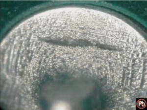
Soldering Anomalies-Hot Tear/Shrink Hole

Acceptable-Class1,2,3
.For connections made with lead free alloys:
.The bottom of the tear is visible.
.The tear or shrink hole does not contact the lead,land or
barrel wall.


Defect-Class 1,2,3
.Shrink holes or hot tear in connections made with SnPb  
solder alloys:

.For connections made with lead free alloys:
.The bottom of the shrink hole or hot tear is not visible.
.The tear or shrink hole contacts the lead or land.
p20s1

                                   end

Frequently Asked S-600-OF Pick & Place Radial Component machine Questions and Answers

What components can the S-600-OF place?

The  S-600-OF  can place components ranging from 0402-??mm2 .  

Radial Leaded components 

Package range is 

What is the minimum/maximum PCB size?

 S-600-OF  can populate a 2″x2″ (50mmx50mm)/15″x18″ PCB(381mmx460mm)

Thickness range: 0.5mm-5.0mm

Weight is restricted to 3.3 lbs. maximum (completed PCB)

What is the topside/bottomside PCB clearance?

Maximum component height is o.256″(6.5mm)

Bottomside clearance is 30mm under the PCB

1. What will be assembled?

2. How much of it will be assembled?

3. How fast must it be assembled?

4. What operations must be performed?

5. In what order should those operations be completed?

6. Can the product design be adapted to accommodate automation?

7. Where are the “trouble spots” in how the product was previously assembled?

8. How well do the parts and components meet tolerances?

9. What Quality standards does the part have to meet?

10. Is there enough space for the equipment?

11. What kind of environment will the equipment be in?

12. How much money is available to spend and When?

13. Will workers need to be hired to run and maintain the equipment?

14. Will workers need to be reassigned?

15. Will the machine be located in another country?


Auto Insertion machine Tooling Design vs. Range of Inserted Component Wire

1.0 INTRODUCTION

Do you have customers who are willing to simplify the Axial automated insertion process, speed up machines, lower preventative maintenance (pm) downtime and ppm levels and generally reduce manufacturing costs?  If so, then this paper may interest you.

Universal Instruments Corporation is currently working to customize tooling for customers who have evolved their manufacturing processes to two and three step processes for Axial insertions, thereby dedicating machines to run a limited range of components.  In step one for example, a machine inserts only 5mm insert spans and then in step 2, a second machine inserts various wire diameters.  This is a radical change from the current manufacturing philosophy of fully populating a board in one pass through a machine.  However, history has shown that by limiting the range of wire diameters inserted and then designing tooling to specifically handle that range, the manufacturing process becomes more controlled, insertion performance improves, pm downtime and ppm levels decrease and ultimately, manufacturing costs decrease.

Admittedly, this approach is not viable for every customer.  Universal offers a variety of tooling configurations that if used according to specification, will provide excellent insertion performance.  A customer may have no need to run a wide range of wire diameters or they may want to revisit their manufacturing process to make improvements.  For those customers, Universal offers customized tooling for dedicated applications.  Customized tooling will handle a limited range of wire diameters to optimize insertion performance and maximize tooling life.

This paper discusses the relationship between tooling design and  wire diameter range of inserted components with the goal of creating an awareness and understanding of this relationship and it’s significance.

2.0 FACTORS AFFECTING THIS RELATIONSHIP

2.1 Depth of V-Groove of Outside Former

One important factor affecting the relationship of tooling design and range of insertable wire diameters is the depth of the V-groove of the Outside Former.  Our current specifications for Axial tooling are as follows:

Standard

High Density

Large Lead

5mm

26mm AAA

Bottom View of Outside Former


Wire Diameter Range / Material

Steel:

.015”-.032”

(.39) – (.82)

Copper:

.015”-.032”

(.39) – (.82)

Steel:

.015”-.025”

(.39) – (.64)

Copper:

.015”-.032”

(.39) – .82)

Steel:

.025”-.032”

(.64) – (.82)

Copper:

.025”-.042”

(.64) – (1.01)

Steel:

.015”-.025”

(.39) – (.64)

Copper:

.015”-.028”

(.39) – (.72)

Steel:

.015”-.020”

(.39) – (.51)

Copper:

.015”-.024”(.39) – (.61)

Driver Tip Width

.030”

(.77)

.030”

(.77)

.050”

(1.27)

.017”*

(.44)

.012”*

(.31)

Metric equivalents are bracketed

* Not entire width but dimension from edge of Driver Tip to side of Outside Former

When the wire diameter is smaller than the depth of the V-groove of the Outside Former, the lead has excess space and moves within the V-groove.  This uncontrolled condition leads to a ‘weak’form. 


 V-groove with Small Lead Diameter

When the wire diameter is larger than the depth of the V-groove of the Outside Former, the yieldable Inside Former flexes to make room for the bigger lead.  Continual flexing causes the O-rings to wear out which leads to a ‘sloppy’Inside Former and ‘weak’forms.  Outside Formers have been known to split at the V-groove from continual stress.  Long term, continual flexing will damage the Tooling Housing by loosening it and making it ‘sloppy’.  


 V-groove with Large Lead Diameter

The optimal condition is wire diameter equal to the depth of the V-groove of the Outside Former.  In this condition, the lead is large enough so that is does not ‘move’within the V-groove, and yet it does not continually flex the Inside Former.


 V-groove with Optimal Lead Diameter

When Standard tooling is compared to 5mm tooling, it becomes clear why 5mm tooling is less reliable when inserting components with large lead diameters than Standard tooling.  

TOOLING

DEPTH OF V-GROOVE

WIRE DIAMETER RANGE

Standard

.028”(0.71mm)

.015”-.032”(0.39mm – 0.82mm).

5mm

.018”(0.46mm)

.015”- .028”(0.39mm – 0.72mm)

The depth of the V-grooves vary by .010”(0.26mm) and yet the range of wire diameter is very similar.

2.2 Radius of V-Groove of Outside Former

Another factor is the radius of the V-groove of the Outside Former.  The V-groove is actually a radius of .016”(0.41mm) for all tooling types except large lead tooling which is .019”(0.49mm).  Because this is a radius, not a diameter, the optimum lead size for this size radius is .032”(0.82mm)  This radius creates a situation that allows a small wire diameter to ‘roll around’or be uncontrolled in the groove.  A true V-groove improves this condition by creating a 2 point contact.  


One Point Contact

Two Point Contact


2.3 Body Length to Insertion Length

Body length to insertion length is another critical issue in this discussion.  The bigger the gap between the component body and the bend of the lead, the more room there is for the insertion tooling.  As the Driver Tip descends, it can damage a component body that is too long for the specified insertion span.  Clearance is also needed for the Inside Former coming beneath the bend of the lead.  A bend too close to the component body can also cause damage.  Maximum body length is obtained with the following formula: 

Programmed Z-Span = Insertion Span + 1 Lead Diameter

Maximum Body Length (clearance between Driver Tips)

= Insertion Span + 1 Lead Diameter – 2 x Depth of Outside Former V-groove – 2 x Driver Tip Thickness 

Do not use components with body lengths at the maximum length.  Allow .020”(0.51mm) on each side of a component body for clearance and to account for tolerances.


Component Body Leaving

Clearance

Component Body Leaving

No Clearance


2.4 Driver Tip Position

During a component insertion, the Driver Tip rests on the horizontal surface of the lead.  When a lead has a ‘weak’form, the Driver Tip rests on top of the bent portion of the lead.  As the Driver Tip tries to push a component through the holes of the pc board, it has a tendency to ‘slide off’a lead, leading to a standup or failed insertion.  This is true of 5mm tooling because of its small Driver Tip.


Driver Tip Position

during insertion

Driver Tip position during insertion 

of weak form lead


3.0 SUMMARY OF ABOVE CONDITIONS

· Wire diameters significantly smaller than the depth of the V-groove of the Outside Former are uncontrolled within the V-groove.  This is caused by one point contact and excess space, which leads to a ‘weak’form and poorly controlled insertion.  Small lead components without a ‘crisp’form are also at risk of misinserting because the Driver Tip may ‘slip off’the lead, while pushing it through the pc board.  This condition is seen most often with 5mm tooling.

· Wire diameters significantly larger than the depth of the V-groove of the Outside Former continually flex the yieldable, Inside Formers causing premature tooling wear-out of the Inside and Outside Formers as well as other parts of the tooling.

· Acceptable component body length varies with Z-span, but clearance is required for the Inside Formers and Driver Tips during insertion so the component body is not damaged. 

4.0 OPTIMAL CONDITIONS

To optimize insertion performance and maximize tooling life, it is best to limit the range of wire diameters inserted with any tooling selection, keeping in mind the optimal wire diameter is the same size as the V-groove of the Outside Former.  For example, if the wire diameter range of a particular application is .018”- .022”, a .020”V-groove is optimal.  This eliminates the problems mentioned above and allows optimal tooling life, process control and low insertion ppm.  

Making use of the squeeze function when writing pattern programs can also help.  If a component lead diameter is small in relation to the V-groove of the Outside Former, the squeeze function can improve a ‘weak’form.  The squeeze function is also useful when inserting steel leaded components as they tend to have a memory after the forming process.  It also helps insert components with long bodies and a small insertion span.

Allow clearance on each side of a component body so there is room for the insertion tooling.

Consider dedicating a manufacturing line to a particular application for optimal performance and then customize the tooling for a small range of wire diameters.  Universal offers customized tooling for dedicated applications.  Customized tooling can include the following items, as needed:

2 point contact in V-groove of Outside Former based on an optimum lead diameter

Increase size of Outside Former footprint for a more robust design

Improved bent lead input insertion capability

UIC TDK SMT,THT,PCB,PCBA,AI. SMT nozzle. SMT feeder. AI spare parts.

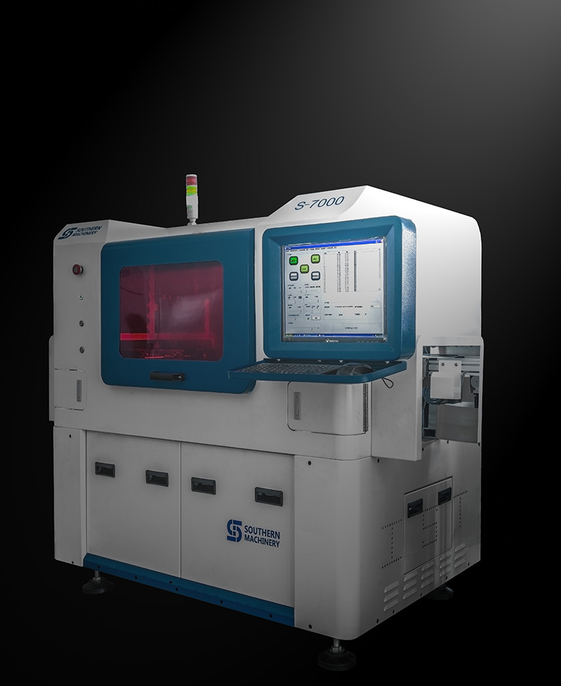
S-7000 Full Automatic Pin Inserter

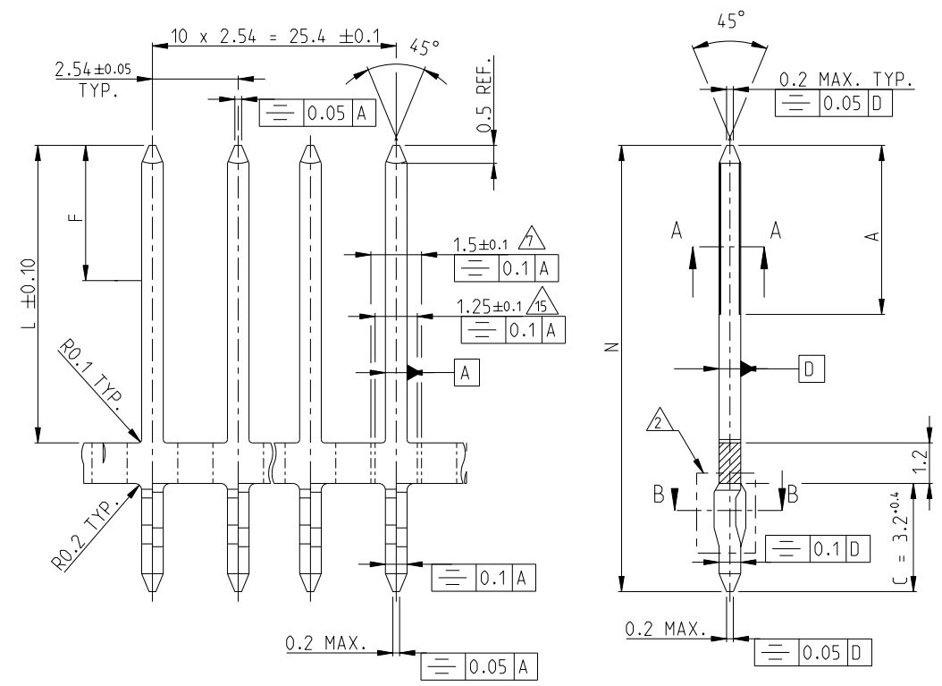
The S-7000 pin inserter  is a custom-made model for square pin insert.

PC control,servo motor drive,vision programming.SMEMA connector.

UIC TDK SMT,THT,PCB,PCBA,AI. SMT nozzle. SMT feeder. AI spare parts.  

UIC TDK SMT,THT,PCB,PCBA,AI. SMT nozzle. SMT feeder. AI spare parts.

UIC TDK SMT,THT,PCB,PCBA,AI. SMT nozzle. SMT feeder. AI spare parts.

Speed 

12,000 CPH Spec

PCB Size

Max. 480mm * 480mm

PCB Thickness

0.76-2.36mm

Insert Head

1

Machine dimension

2300mm*1340mm*1860mm (L*W*H)

Machine weight

1500KG 

Power supply

Single Phase 220VAC, 50/60HZ, 1.0KVA

System Protection

UPS

Air pressure

0.4-0.6Mpa (Round pin 0.55-0.6Mpa)/0.3M3/Min

Data input

USB interface input (EXCEL format)

Control System

English version interface (WINDOWS system control platform) LCD monitor

PCB transfer mode

automatic load / unload

UIC TDK SMT,THT,PCB,PCBA,AI. SMT nozzle. SMT feeder. AI spare parts.

Want more information,pls leave a comment

5 Reasons for you to choose LED SMT assemble line from Southern Machinery

24 hours online service for LED SMT assembly machines:

S-K100 LED line

1)What is high speed SMT pick and place machine ?

The high speed automatic SMT mounting machine is the equipment used to realize high-speed, high accuracy completely automatic mounting the electric elements like LED light sphere, electric resistance , electric capacity etc. It is the mot essential and most complex equipment in the entire SMT production. The mounting machine is the major machine in SMT production line, and it is already developed from the early low speed mechanical mounting machine to high-speed optics mounting machine, and to multipurpose, flexible connection modulation development.


2)What machines does the LED board processing need ?

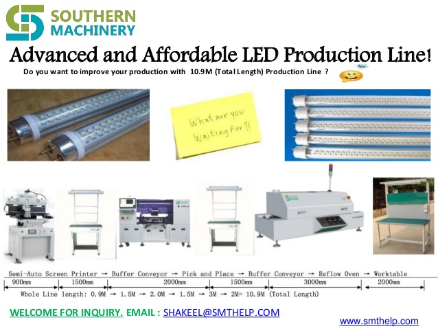
The LED mount technical process simplification is: Printing, Pick and placing, Reflow Oven (in each part, you can join examine link to control quality)


3) What are the advantages of Southern Machinery SMT pick and place machine ?

a.Top high speed in the world, quick than the main SMT machines brands like Siemens, Fuji, Samsung, Panasonic, Sanyo;

b.Lowest power consumption, 2.5-3.5KW/Hour;

c.Match vacuum pumps along with the main machine, no need to match extra vacuum pump;

d.Electric control system is installed on the top of the main machine, easy to maintain, and has a good damp proof effect;

e.Integrated forming steel frame, guarantee our mounting machine a stable performance on high speed running conditions.

f.The distance of sucking mouth can be adjusted manually, photoelectric will make sure the accuracy after adjust, allow you to mount different pitches PCB board.


4) What kinds electric elements can use our high speed SMT machine !

The main elements our machine can mount include: LED lights, electric capacity and electric resistance, sizes like: 0805,1206,2121,2835,3014,3528,5050,5630,5730,RGB; mainly for 1.2-1.5 meter LED light tube, LED panel light, 0.5-1.0 meter LED light strip , RGB strip.


5) What is our main business scope ?

We are the leading manufactuer of SMT LED mounting machines in Shenzhen, China, and we can produce and supply you all the SMT processing needed machines to you, mainly include: LED PCB board mounting machine, PCB board printer, PCB board reflow oven , and other related SMT devices.


For more detailed information about our  LED SMT assemble line, email us freely, and you are warmly welcomed to visit our factory for SMT devices business !

What service you can enjoy if you purchase   machine from us:

  • 1. AI/SMT PCB Design Guidance

    • How to improve machine’s efficiency,save more workers for you.
    • Starting from the PCB layout and component specifications.
    • Considering the potential of equipment, 
    • how to make the machine’s actual speed to be theoretical.PCB size ,
    • how to custom can make more efficient
  • 2. AI/SMT Technology Process Of Import

    • First insert or pick&place?Step-by-step to guide you for designing your PCB production process.
    • The new product programming, transfer line, how to deal with many varieties of small batch ?
    • How to reduce the production process defective rate?
    • Improve the continuous optimization
  • 3. Equipment’s installation And Technology Training

    • What position does your equipment should be installed in the workshop?
    • Teach you how to layout the workshop for most conforms  the technological process, save workers.
    •  Care about the more precise assembly and installing your equipment more than you.
    • Equipment installation before/after have comprehensive training courses.
    • We have English training courses and years of experience to install abroad.
    • We not only training the AI/SMT machine, we study together, progress together.
  • 4. Machine Trouble Shooting/Retrofit/Overhaul/Relocating

    • Equipment production status 7X24 hours in the Cloud End, managers “anytime” “anywhere” insight into equipment production, state;
    • Factory technical experts can 7 x24 hours online video consultation equipment technical fault, the cloud initiative to monitor and remind equipment maintenance;
    • We upgrade your machine, you increase your productivity;
    • And maintenance of the annual/full access to our professional engineer, they well, you must be able to get beyond your expectations of harvest;

  • 5. AI/SMT Machine Accessories

  • Equipment 7 x24 hours in the “cloud”, we offer equipment spare parts list according to equipment real-time state, and supported the use of PC equipment direct orders to buy;  
  • We have many years of AI/SMT machine accessories design, production and manufacturing experiences;
  • We service life of spare parts, as well as spare parts affect the quality of the products for machinery and equipment and , and that, we willing to help our customers;
  • We not only provide wearing parts replacement, more willing to provide you with technical guidance;
  • We have professional engineers to electronic boards, motors and so on to provide maintenance services.

SMT,THT,PCB,PCBA,AI,wave soldering,reflow oven,nozzle,feeder,wave soldering,PCB Assembly, LED, LED lamp, LED display,

“S-EF 3000 S-A Pick & Place Machine for Led Lighting ” Best Quality – Affordable Price !

“S-EF 30000 Semi-automatic pick & place machine for led lighting Products.”

SMT,THT,PCB,PCBA,AI,wave soldering,reflow oven,nozzle,feeder,wave soldering,PCB Assembly, LED, LED lamp, LED display,