AI spare parts、Universal Parts,UIC,TDK.VCD Sequencer.SMT,THT,PCB,PCBA,AI,wave soldering,reflow oven,nozzle,feeder,wave soldering,PCB Assembly, LED, LED lamp, LED display

One Video show you how to auto insertion Odd form Component for Electronic manufacturing

PCBA Auto Insertion  – Axial, DIP, Radial, Pin, Odd-Form

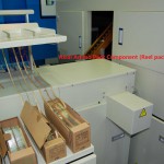
We design and manufacture Odd Form component auto insertion machine,SMT equipment, and providing spare parts service. Worldwide Installation and on site support and training.

The primary sources for (new) automated through hole component insertion or through hole component assembly equipment today, are: Contact Systems, Fuji, Panasonic, TDK and Universal Instruments. All (5) OEMs have contributed to the advancements in equipment and technology that we use today to assemble printed circuit boards, and all provide spare parts and varying levels of technical support.


Contact System’s semi-automatic component insertion systems are capable of processing a wide range of components, including: axial, radial, dip, sip and even many odd-form devices. Although Contact’s machine are most commonly used to augment fully automatic assembly processes, it is not unusual to see the Contact Systems CS 400D and CS 400E component locators being used as the primary means of assembling printed circuit boards at many low to moderate volume manufacturing facilities. All CS 400 systems are ergonomically designed to minimize operator fatigue and maximize productivity by combining a convenient operator to machine interface with several types of parts delivery systems, including their: CS 210 Rotary Bin, CS 400LPD – Large Parts Dispenser, CS 241 Lighted DIP Dispenser and the CS 740 JIT Component Delivery Systems which are available in single ( CS 740BS ) and double picker ( CS 740BD ) configurations.

Contact System’s Ultra Clinch offers the unique feature of allowing the user to program lead lengths and clinch angles for each and every component being assembled.

Component insertion rates of 600 pph to 1,500 pph are typical.

Universal Instruments Corporation manufactures a complete line of through hole insertion equipment. Also known as Insertion Mounted Component ( IMC ) and pin in hole assembly equipment, UIC offers automatic component insertion platforms for: Axial, DIP, Pin, Radial, SIP, LED, Transistor and Odd-form devices.

Universal’s IMC line of axial component processing equipment includes:

Axial component sequencers that are available in the following models: 2596R, 2596A, 2596B, 2596C and 2596D. The expandable axial sequencers can be configured with: 20 to 220 stations using (20) station add-on modules, expanded range verifiers (ERV), refire, pass-thru or single board transfer – SBT . The typical yield rate of a Universal sequencer ranges from 12,000 pph to 25,000 pph.

To compliment the 2596 sequencer, Universal offers the following axial component insertion systems: 6285, 6287, 6287A, 6287B, Generation 8, VCD single head 8 and model 6295 dual head VCD. Other VCD based inserters include the Jumper wire single head 8 and Jumper wire dual head 8. The cycle rates of these machines range from 8,500 pph to 40,000 pph depending on their configuration and vintage. Aside from cycle rates their operating parameters are similar.

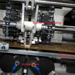
As an alternative to stand alone equipment, Universal also offers a combined sequencer/inserter for axial leaded devices. Referred to as: 6241, 6241A, 6241B, 6241C, 6241D, 6248/48F, VCD Sequencer 8 Inserter, these axial lead sequencer / inserters can be configured with the same features as stand alone equipment.

Universal’s DIP Inserter product line include: Uni-module, Multi-module and SIP platforms. Available options include: 4 Pin DIP LED Tooling, DIP/Socket tooling, Autostick, and Single Board Transfer. The single head Uni-mod or model 6796 will typically yield 2,500 pph to 3,200 pph. The dual head Multi-mod or model 6772 typically yields 3,400 pph to 4,200 pph.

Universal’s Radial Sequencer/Inserter product line inserts radially taped and reeled components with body diameters up to 13mm and lead spans of 2.5/5mm at speeds ranging from 6,500 pph to 11,000 pph. Often referred to as Rad 1, Rad 2, Rad 3, Rad 5 and Rad 8 machines, these platforms can be configured with: 20 to 80 stations, single board transfer – SBT and expanded range verifiers – ERV. Model numbers associated with the Radial products include: 6346, 6348, 6358, 6360 and 6380.

Fuji, Panasonic Factory Automation and TDK offer competitive products, including: Fuji’s Flexible Board Assembler – FBA, Panasonic’s RH & AV and TDK’s RH.


AI spare parts、Universal Parts,UIC,TDK.VCD Sequencer.SMT,THT,PCB,PCBA,AI,wave soldering,reflow oven,nozzle,feeder,wave soldering,PCB Assembly, LED, LED lamp, LED display AI spare parts、Universal Parts,UIC,TDK.VCD Sequencer.SMT,THT,PCB,PCBA,AI,wave soldering,reflow oven,nozzle,feeder,wave soldering,PCB Assembly, LED, LED lamp, LED display AI spare parts、Universal Parts,UIC,TDK.VCD Sequencer.SMT,THT,PCB,PCBA,AI,wave soldering,reflow oven,nozzle,feeder,wave soldering,PCB Assembly, LED, LED lamp, LED display AI spare parts、Universal Parts,UIC,TDK.VCD Sequencer.SMT,THT,PCB,PCBA,AI,wave soldering,reflow oven,nozzle,feeder,wave soldering,PCB Assembly, LED, LED lamp, LED display

AI spare parts、Universal Parts,UIC,TDK.VCD Sequencer.SMT,THT,PCB,PCBA,AI,wave soldering,reflow oven,nozzle,feeder,wave soldering,PCB Assembly, LED, LED lamp, LED display

S-ws250 Wave soldering machine for electronic manufacturing PCBA

Lead-free or Tin-lead Through-hole Soldering

adjustable dual waves permit lead-free or tin/lead processing of through-hole and SMD boards to a maximum width of 250 mm

As PCBs are loaded onto the adjustable titanium finger conveyor, they are automatically prepped by an adjustable internal spray fluxing system which houses a precision spray nozzle assembly mounted to a reciprocating Y-axis drive mechanism to ensure even and accurate application of flux.

Run as Dual or Single Wave

Solder processing temperature is settable to a lead-free compatible 300°C. The system includes an economical low-volume 200 kg (550 lbs. Approximate weight for lead free solder) capacity solder pot with an easy-handling roll-out feature. A built-in alarm signals when solder level is at the refill point.

Forced Hot Air Convection Pre-Heat

The preheat stage takes place in a 600 mm (23.6″) glass-covered chamber where boards are heat-bathed by energy-saving forced hot air convection, as opposed to power-consuming, uneven IR heat.

AI spare parts、Universal Parts,UIC,TDK.VCD Sequencer.SMT,THT,PCB,PCBA,AI,wave soldering,reflow oven,nozzle,feeder,wave soldering,PCB Assembly, LED, LED lamp, LED display


Automatic spray fluxer produces uniform fine spray coverage of underside of each incoming board. Integrated cooling zone provides rapid cooling for processed boards prior to exiting the conveyor.
Energy-conserving 600 mm (23.6”) forced hot air convection preheater safely preps boards for higher temperatures of lead-free or tin-lead soldering while ensuring that fluxes are properly activated. Process area—where dual waves are generated by titanium alloy wave nozzles.
Preheat area remains enclosed under glass during processing, preventing escape of hot air. With front panel removed, dual solder pumps (top) and solder pot below are exposed. Electrical panel is accessed by removing cabinet door on right side.
Cooling fans apply focused below-board heat to quickly lower temperatures of processed boards. Titanium-alloy wave nozzle and components resist corrosion. Finger conveyors are automatically cleaned prior to loading of each board.
Titanium finger conveyor is hand-crank adjustable to boards of up to 350 mm width. Titanium finger conveyor is hand-crank adjustable to boards up to 350 mm width. Fingers are self cleaning.
Built-in flux fume exhaust hood and filter. Flux vapors are extracted through a built-in fume hood and filter, and out of the system through an exhaust flange on the top of the unit. The filter is easily removable for cleaning. A tote case containing all hand tools necessary for maintenance, repair or disassembly

Universal Auto Insertion Machine Axial Inserter ^241F PC BOARD FUNCTIONAL/TEST SPECIFICATION

PC BOARD FUNCTIONAL/TEST SPECIFICATION

DESCRIPTION OF ASSEMBLY PCA, SEQ MMIT I/O

PART NUMBER OF ASSEMBLY 47634502, -03, -04

PRODUCT CODE(S) 6241F

RELEASE NUMBER 66764/1018294

RELEASE DATE 4/15/10 (Updated 2/24/10)

  1. product description overview
  1. introduction

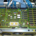
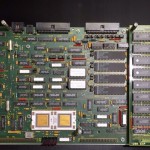
The Sequencer MMIT I/O Assy replaces the sequencer I/O box, the Optical Refire controllers, and the 20 AC Out PCBs with a single I/O card that interfaces to the Mini-MIT bus that has been used on the SMT Platform since its inception. The card has 20 DC outputs capable of driving up to 1 amp each at 12 VDC. The card has 40 inputs that are nominally dedicated for low parts and parts missing for the dispensing heads. In addition, the card has a diagnostic port which is not connected to any outputs and 8 general purpose inputs and outputs for other features such as start and stop switches.

  1. history

This card is a new design, but based on experience with Mini-MIT on the platform. The functions of this I/O card are the same as those of the modules it replaces (refire controller, 20 AC Output).

  1. physical description

The card is the same size as the 20 AC Output (5”x15”). The construction is a multi-layer surface mount assembly. To streamline manufacture, as many of the components as possible are surface mount.

  1. Compatibility

This card is designed to completely replace the previous control scheme. The only compatibility to existing equipment is for the dispensing heads and the jumper wire feeder. This card will support the new (stepper controlled) or old feeder. The cabling to the jumper wire feeder, however, is different. This card will not support the older AC valves or the old Refire Det PCBs. DC valves are required and the new Refire Det PCA is needed.

  1. operating features

The Seq MMIT I/O PCA an I/O card optimized for use on the IM sequencers. It has separate connectors for Mini-MIT in and out, and has separate connectors for each of the functions supported. In this way, the cabling can be modular, avoiding massive cable harnesses. All signals are routed through the gate array, which is programmable. Thus, the card’s function can be tailored to suit many diverse needs. The card is designed for low power consumption which reduces the cost of cables and eliminates any thermal problems. All signals going off board are conditioned to protect the board from damage from accidental wiring errors.

  1. operating specifications
  1. electrical power requirements

ï +12 VDC @ 4 A max.

ï +5 VDC @ 2 A max.

ï 24 VAC @ 2.5 A max.

Over current protection for the main +12 VDC and +5 VDC are provided by the power supply. The power supply should not be replaced without due consideration to the over current protection.

  1. Thermal considerations

There are no reasons for concern for any expected thermal conditions in the environment that it will be used in.

  1. inputs

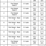
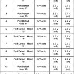
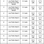
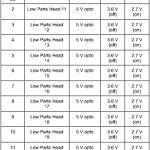
There are 48 inputs that are optically isolated and filtered. These are used for (20) part missing, (20) low parts and (8) general purpose inputs.

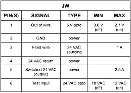
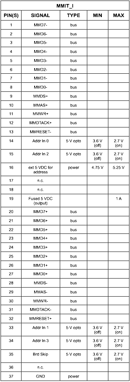
  • 5 V OPTO: Inputs are optically isolated with noise rejection. The input signals are referenced to the local +5 VDC supply. The inputs must be pulled below 2.7 VDC (2.3 VDC across the input) to activate the input. To guarantee the inactive state, the input must be above 3.6 VDC. There is a 0.01?F filtering capacitor across the opto-coupler to filter out high frequency noise. In addition, there is debouncing in the gate array to weed out signals shorter than approximately 50 ?s.
  • 12 V OPTO: Inputs are optically isolated with noise rejection. The input signals are referenced to the local +5 VDC supply. The inputs must be pulled below 9.2 VDC (2.8 VDC across the input) to activate the input. To guarantee the inactive state, the input must be above 10.3 VDC. There is a 0.01?F filtering capacitor across the opto-coupler to filter out high frequency noise. In addition, there is debouncing in the gate array to weed out signals shorter than approximately 50 ?s.
  • 24 VAC OPTO: There is one input referenced to 24 VAC for the TEST input from the jumper wire feeder. This input is diode blocked to provide a pulsing signal. There is one pulse per AC cycle. The input pulses are stretched in the gate array to approximately 27 ms. The input line must be pulled below 12 VACrms to guarantee an active signal and must be above 18 VACrms to guarantee an inactive state.
  • TTL INPUT: This is used only for a jumper in the plug that connects to this board to indicate that it is plugged in. This signal does not go off board any distance.
  1. outputs

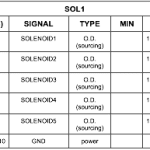
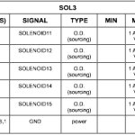
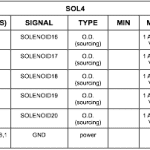
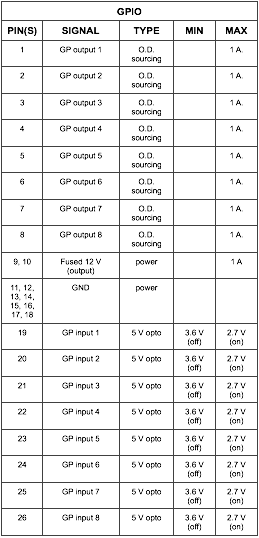
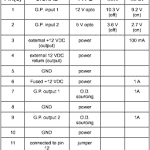
There are (20) 12 VDC sourcing outputs for valve solenoids. Each is capable of driving up to 1 A. There are 8 general purpose outputs that are also 12 VDC sourcing. In addition, 5 of these general purpose outputs also have AC relays on them capable of sourcing 24 VAC at up to 1 A.

  • O.D. SOURCING: Open drain MOSFET output referenced to the local +12 VDC supply. They are capable of sourcing 1 A each. The total limit of the 12 V supply is 4 A.
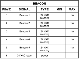
  • 24 VAC SOURCING: Triac output supplies 24 VAC at a maximum of 1 A.
  • O.C. Sinking: Open collector TTL output (7407) referenced to the 5 VDC return (GND). These outputs are used for data links to adjacent boards.
  1. connector pin out

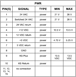
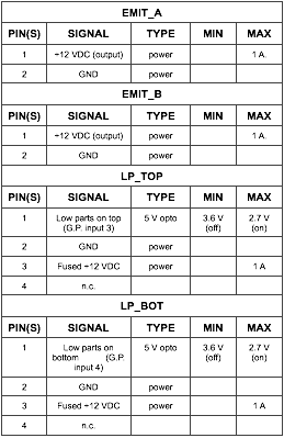
Power Input: 15 pin AMP Mate-n-lok connector that supplies +12 VDC, return, +5 VDC, return, 24 VAC, switched 24 VAC, and return, and an external power source.

Jumper Wire Feeder: 6 pin AMP Mate-n-lok connector that supplies 24 VAC, return, the DC output for head 3 and the Out of Wire input for head 3. The output and input are in parallel with the output and input for the dispensing head itself. In addition, there is a Test input from the jumper wire feeder that will manually feed a wire and fire the dispensing head.

Valve Drivers: (4) 10 pin Mod-U connectors supplying 5 sourcing signal lines and 5 return lines. These outputs are open drain P-channel MOSFETs.

Part Missing: (2) 15 socket D-Shell connectors supplying 12 VDC, Return, (10) input signal lines, and a control line for the test function.

Low Parts & Dual Part Sensor: two 25 socket D-Shell connector that supplies 12 VDC, Return, and ten input signal lines each.

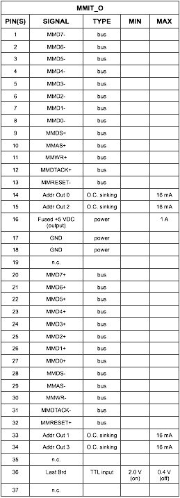
Mini-MIT input: 37 pin D-Shell that contains the (13) Mini-MIT pairs of lines as well as four lines to determine address and one line to determine if the previous board was bypassed. These inputs are optically isolated and receive their power from the previous module. There is also a +5 VDC line provided for powering the first module’s input.

Mini-MIT output: 37 socket D-Shell that contains the (13) Mini-MIT pairs of lines, four outputs for address, an input to indicate additional cards follow, and a jumper to differentiate from a bypasses card. If this is the last card in the chain, a terminator plug must be inserted into this connector.

General Purpose I/O: one 26 socket D-Shell connector that supplies 12 VDC, Return, (8) input signal lines, and (8) sourcing output signal lines.

Low Parts Scanners: Two 2 pin AMP Mod-U connectors that have +12 VDC and return to power the light sources. Also, two 4 pin AMP Mod-U connectors to power the receivers and to receive the signal.

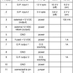
Push Buttons: Two 12 pin AMP Mate-n-lok connectors that have +12 VDC and return, an external +12 VDC and return, and two inputs and two outputs.

Beacon: The upper http://buyclomidovulation.com five outputs of the general purpose group also have AC relays that can be used for a beacon. These outputs are on a 6 pin Mod-U connector. These outputs use separate logic out of the gate array and can be re-programmed to operate separately from the general purpose I/O.

6) indicators

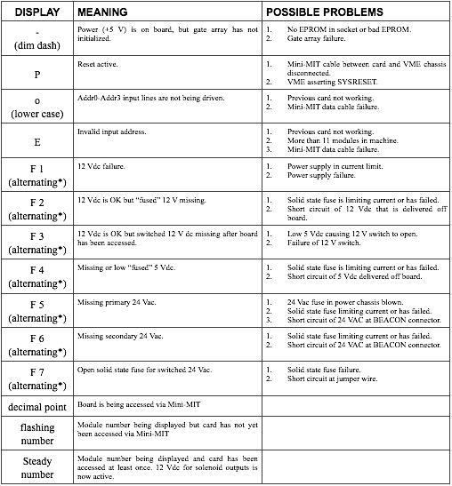
The board does not have any LED indicators on any of the inputs or outputs. There is a single digit 7 segment display that will display the address of the card or a fault code. The chart below describes the display.

* – alternating means that the F will appear for 500 milliseconds, then the fault code number will appear for 500 milliseconds, then repeat.

  1. theory of operation

All signals go through the Gate Array (U27). The gate array provides all of the logic necessary for decoding the bus signals, providing any latches or counters necessary, and providing the output signals. The only external components are the interface chips to provide the RS-485 interface, the opto-couplers for the inputs, and the high current drivers for the valves, etc. The logic in the gate array is loaded on every power up and is stored in an 8 pin EPROM (U18) that resides in a socket on the board.

  1. Mini-MIT interface

The card is programmed to respond to four different address ranges: (1300h + “card address” * 10h) is the base address for the valve outputs; (1306h + “card address” * 10h) is the base address for the part missing and low parts inputs; (13C0h + “card address” * 4) is the base address for the diagnostic port and general purpose I/O; and 13FEh on the last module will respond with the size of the sequencer.

  1. card addressing

The card addressing is accomplished with four bits that are passed into and out of each card. These are on pins 14-16 and 33-35 of the Mini-MIT connectors. Four of these lines make up an address. The first module will see all of these lines low when plugged into the inserter. Each card will take the number passed into it, add one, and use that as its address. Each card will pass its address out to the next card. In this way, the first card will see 0, and, adding one, will use an address of 1. This 1 will be passed on to the second card, which will add one to it and use 2 for its address. This process will continue until all the cards have a unique address. These bits are constantly updated (i.e. can dynamically change) until the card is addressed for the first time after power up or reset. At that time, the display will stop flashing and will display a solid digit, which is its address. If a reset occurs, the display will start flashing again, and the address becomes dynamic again, until the card is again accessed. Reset is accomplished globally over the Mini-MIT bus or by cycling power.

There are additional wires in the Mini-MIT cable to determine when there is a cable plugged into the output connector (as opposed to a terminator). This will allow the last card to respond to address 13FEh to provide the size of the sequencer (the number of modules).

There is also a connection on the board to differentiate between a single cable connecting adjacent cards as opposed to two cables in series between adjacent cards. The two cables would only be used if there was a defect in one of the Mini-MIT I/O cards and it was necessary to bypass it. In this case, the card will add 2 to the incoming address instead of just 1. In this way, all subsequent modules will still have their correct addresses. It must be noted that this bypass procedure will only work with one card bypassed. Two adjacent cards cannot be bypassed in this way.

  1. diagnostic port

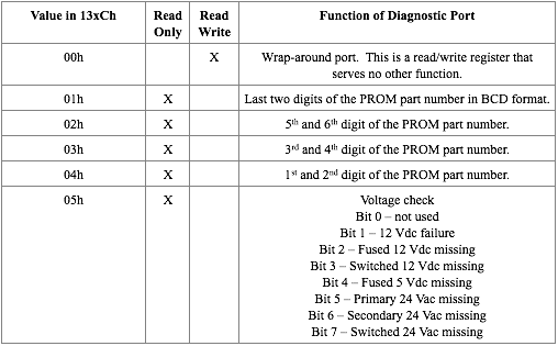
This is an 8 bit read-write register (at 13C2h + “card address” * 4) that can be used to access various diagnostic features. The function of this port is defined by writing to a write only register (at 130Ch + “card address” * 10h). The following chart outlines the currently implemented features.

  1. part missing inputs

The part missing inputs are latches that are active while the corresponding valve output is active. The latch gets cleared on the leading edge of the valve output. If an input occurs during the time that the output is active (indicating a part present), the latch will be set until the next time that head is fired. The machine controller can read the status of that bit at any time thereafter until the next time that that head is fired.

For troubleshooting purposes, there are three test functions that can simulate the function of the part missing (refire) sensors built into the dispensing heads. Writing a 1 to 13x6h (where ‘x’ indicates module number) clears all of the part missing latches. Writing a 1 to 13x8h issues a 2 ms pulse to the refire boards to simulate a part present in the head. A head must be plugged into the refire jack for this function to test all of the hardware. Writing a 1 to 13xAh enables all of the latches for 2 ms without sending a test pulse to the refire boards. This function makes sure that the latches are not stuck in the active state. A working dispense head must be plugged into the refire jack for this function to operate.

  1. output drivers

The output drivers are optically isolated from the gate array and are SOURCING of 12 VDC (or of 24 VAC in the case of the AC outputs). The outputs are held in a disabled state during power up and until the card is addressed for the first time. This will avoid any possibility of a power up glitch.

  1. optically isolated inputs

The inputs are all isolated from the outside world by opto-couplers. The input section is designed to be used with a 12 VDC reference. It consists of a voltage divider with a small bypass capacitor. This prevents any low amplitude or high frequency noise from causing an input to be registered.

7) VCD DUAL PART SENSOR INPUT

Two optically isolated inputs, LPA pin 1 and LPA pin 2 are used in the dual part sensor application. These sensors inspect for two parts in the chain clip. The counting of the parts is generated in the FPGA, and provided out of the MMIT bus.

In the FPGA, each channel for the dual part sensor counts independently. The MMIT output value that is read is the maximum of these two summed values.

This count can be found by reading bit locations 7,6,5 of the 0x13x4H MMIT address. By writing these bits, the register count is Reset. Bit location #4 is the immediate value of the sensor.

  1. Adjustments

There are no adjustments or setups on this card. The card addressing is automatic. If it becomes necessary in the future to have option settings, they can be implemented in one of two ways. First, they can be hard-coded into the serial EPROM, which is socketed. Alternatively, option settings can be downloaded to registers over the Mini-MIT bus.

  1. supporting documents
  • 47634502 – Seq MMIT I/O Assembly and schematic
  • 47634503 – Seq MMIT I/O Assembly and schematic
  • 47634504 – Seq MMIT I/O Assembly and schematic
  • 47634403 – Seq MMIT I/O fabrication drawing.
  • 47669101 – Functional Spec for the Refire Det PCA.
  • 44901301 – Functional Spec for MiniMIT TO Assy.

Universal Auto Insertion Machine J11 (8223) controller troubleshooting guide

Document part number 43380001

Revision E

Title 8223 troubleshooting guide

Date February 27, 1996

Engineer R. Lindaman

1 INTRODUCTION

The intention of this guide is to provide a method of diagnosing a problem with a 8223 controller. Due to the close interaction of the controller with the machine it is embedded in, it is often difficult to determine the cause of a problem. Therefore items such as power supplies and cabling are important.

Knowledge of ODT (Digital Equipment Corporations Online Debugging Technique) is essential. See end of guide for command summary.

2 QUICK CHECK LIST

The following are problems that have been observed in the past and should be checked first.

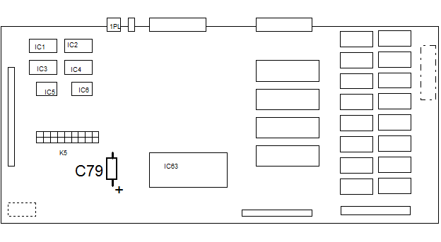
2.1 Power supply voltage must be set between 4.95 and 5.00 volts as measured on J11 ( put meter across C79 on CPU board ). Note the test points on the EMI/PS board do not accurately reflect the supply voltage. See section CONTROLLER POWER, subsection EMI/PS and Appendix A.

2.2 Intermittent power supply connections at rear of DC supply chassis. In particular the 3PL “RED BRICK” style connector which supplies +5,+15,15 volts to the J11 and I/O box. It’s on the rear of the power supply chassis. Due to poor connections at 3PL the J11 receives a low +5 volts. This is applicable to older machines.

2.3 Intermittent or poor connections of power cable to back of I/O box. Cause low voltage to I/O box and J11. This is applicable to older machines. Check the backplane of the I/O box. If there is a small PCB part number 433993xx MIB PWR ASSY, then the connector issues stated above should not be a problem.

2.4 On the J11 CPU board and memory expansion board some IC’s installed in sockets have bent leads. In particular IC19 on the memory expansion board is suspect.

2.5 Open fuses in the memory battery circuit ( 1FU on memory expansion board and 2FU on the J11 CPU board ). J11 CPU part number 433797xx and J11 EXP MEM 43423001 do not have a fuse!

2.6 On the memory expansion board where the battery solders to the PCB there have been bad connections. With an ohm meter the resistance between the negative battery lead and ground ( ground may be any memory IC pin 14 ) it should be a short ( less than 0.1 ohms ).

2.7 A change was made to the EMI/PS board to correct some power down problems. The machine should have a 41693302 PC CD, EMI/PS ASSY as opposed to a 41693301 ( or other ?).

2.8 System powers up properly only every other time ?. Check cable between EMI/PS and J11 CPU board ( 10 wire shielded flat cable ).

2.9 Exec’s 417247xx REV B and 405912xx, 405913xx REV L have a known power down problem. A power fail modified J11 or new exec will fix it.

2.10 If serial communications problem Check IC65, IC66, IC67. The receiver (IC67) is damaged easily by ESD. Some versions have sockets for these ICs making them easy to replace.

2.10.1 IC65 MC1488 or equivalent

2.10.2 IC66 MC3487, 26LS31C or equivalent

2.10.3 IC67 MC3486, 26LS32A or equivalent

2.11 Check jumper configuration against machine documentation.

2.12 Unit goes into ODT and will not properly accept input from the console. IC’s 43 and/or 52 may have failed. See section on IC42 and IC53 for additional information (pre 1990 units)

3 SYMPTOMS

The following are general categories of system failure.

3.1 No communications with console.

3.2 Improper communications with console

3.3 Incorrect communications with console

3.4 Fails to communicate with Host.

3.5 Trap errors.

3.6 Fails to power up in Executive program.

3.7 Losses pattern data

3.8 Incorrect control of machine I/O.

3.9 Repeats outputting the UIC restart message

4 NO COMMUNICATIONS WITH CONSOLE.

4.1 Check controller power. If OK then do next check.

4.2 Check state of J11 CPU PCB’s indicators. If OK then do next check.

4.3 Check console serial I/O.

5 IMPROPER COMMUNICATIONS WITH CONSOLE.

5.1 Check controller power. If OK then do next check.

5.2 Check IC43 and IC52. If OK then do next check.

5.3 Check console serial I/O

6 FAILS TO COMMUNICATE WITH HOST OR OTHER SERIAL I/O

6.1 Check controller power. If OK then do next check.

6.2 Check state of J11 CPU PCB’s indicators. If OK then do next check.

6.3 Check serial I/O

7 TRAP ERRORS

There are two causes of trap errors, hardware failures and software failures. Traps occur due to the program not executing properly which could be a software programming error contents of memory changing or memory failure. Hardware problems will be covered.

The following should be examined in the order given:

7.1 Check controller power. If OK then next step.

7.2 Check memory voltage supply circuit. If OK then next step.

7.3 Check EMI/PS for power timing. If OK then next step

7.4 Check Socketed IC’s. If OK then next step.

7.5 Check memory using PFAIL program.

8 FAILS TO POWER UP IN EXEC PROGRAM.

The causes for this are usually the same as those for trap errors. Follow the procedure for trap errors. Also check IC43 and IC52.

9 LOOSES PATTERN DATA

The causes for this are usually the same as those for trap errors. Follow the procedure for trap errors.

10 INCORRECT CONTROL OF MACHINE I/O

Typically these symptoms are chattering valves, improper DAC outputs, improper encoder values.

The following should be checked:

10.1 Check controller power. If OK then next step.

10.2 Check local I/O

10.3 Check external I/O

11 REPEATS OUTPUTTING THE UIC RESTART MESSAGE

This problem has been observed as being related to controller power. If the + 5 volts at the EMI/PS card is close to the limits at which it detects voltage out of tolerance, this problem can occur. Typically the EMI/PS detects under voltage when below 4.70 volts and over voltage at 5.3 volts. When the voltage is near these limits the system will Reset/Restart as the voltage drifts up and or down slightly.

The PINT indicator on the EMI/PS will activate if this is occurring. See section CONTROLLER POWER, sub section PINT INDICATOR.

11.1 Check controller power

12 CONTROLLER POWER

The following are areas to investigate regarding checking the power that the controller receives from the machine.

12.1 Supply Voltages

Measure power supply voltages at the point indicated. Variations from this should be investigated and corrected. Also see appendix A for additional information.

12.1.1 +5 Volts – The 5 volt test point should not be used for measuring the 5 volts. ( see section on CPU power, subsection EMI/PS ). Measure using one of the following, the voltage should be +4.90 to +5.00 ( VDC ).

12.1.1.1 MIB PWR Adaptor If a MIB PWR adaptor card is installed on the backplane use the Black test point on it ( +5 volt TP ) and the Yellow Ground.
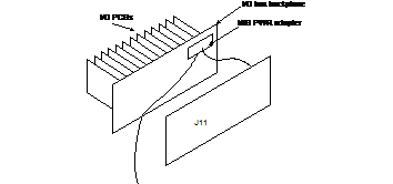
12.1.1.2 C79 On CPU Board – See Diagram no. 1 at the end of this guide for location of C79. When using this point to measure compare this voltage to the 5 volts measured on the I/O box backplane ( use pin 80 for +5 volts and pin 76 for ground ). The difference should be less than 0.1 volts. If it is not less than 0.1 volts then the “Y” adaptor cable that provides power to the I/O box and J11 should be checked for poor connections.
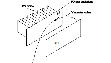
12.1.2 +15 Volts The test points on the MIB PWR adaptor card or EMI/PS board may be used. Brown test point, +14.6 to +15.00 ( VDC )

12.1.3 15 Volts The test points on the MIB PWR adaptor card or EMI/PS board may be used. Red test point, 14.6 to 15.00 ( VDC )

12.1.4 24VAC Use TP4 ( Orange ) on the EMI/PS, 20.0 to 28.0 ( VAC ). The 24 VAC comes through the shielded ribbon cable between the EMI/PS and J11 cpu board then through a fuse on the J11 cpu board then out 9PL of the J11. Check this path if there is no 24 VAC.

12.1.5 General Power Supply Notes The J11 controller is tolerant of variations in the +/ 15 volts DC and 24 VAC but NOT the 5 volts DC. Should the 5 volt supply not be within stated tolerance check the voltage drop of the connector/cables leading from the supply chassis to the I/O box. To do this measure the 5 volt supply at the supply. Typically it is set at 5.5 to 5.6 volts. If the supply is within range but the TP1 does not read the correct value then the cable should be suspect. Wiggle the connectors at the supply chassis, I/O box and Y adaptor cable in back of the I/O box. These have been observed to cause problems. Check the backplane of the I/O box. If there is a small PCB part number 433993xx MIB PWR ASSY, then the connector issues stated above should not be a problem. The DCOK indicator ON the EMI/PS should be on with the supplies are set properly. If the supplies are OK and the DCOK indicators is out the replace EMI/PS board.

12.2 CPU Power – Measure +5 on the J11 controller PCB. Measure at C79. See Diagram no. 1 at the end of this guide for location of C79. Measure +/ 15 on the J11 CPU board.

12.3 EMI/PS

The EMI/PS board ( 41693302 REV A or earlier ) has a voltage drop in the +5 volts between the I/O box side of the board and the test point side. When the test points are used to set the +5 volts ( as has been recommended ) the voltage at the I/O Box can be up to 0.25 volts more. To allow for more accurate setting of the voltage a change has been issued to reduce the voltage drop. 41693302 REV B boards have this change included.

12.4 PINT Indicator

The PINT ( Power INTerrupt ) indicator on the EMI/PS board indicates that the power detector section of the EMI/PS board has detected a interruption of the AC line or a out of tolerance condition of the 5 volt power.

On power up ( assuming power has been off for approximately 15 seconds ) the indicator should be off. Following a normal power up the indicator will stay off until a interruption of the AC line or a out of tolerance condition of the 5 volt power is detected.

This may be simulated by quickly turning the AC power off then on again. If the indicator is on it may be turned off by either turning power off for more than 15 seconds and turning on again or by pressing the small pushbutton on the EMI/PS board.

13 CPU INDICATORS

There are four CPU indicators. Providing that system power is OK then the indicators have the following meaning.

13.1 All On

When all LED’s are on it generally means that the cpu is being held in reset. This may be due to:

13.1.1 System power incorrect ( see section on supply voltages )

13.1.2 Bad EMI/PS board. ON EMI/PS measure IC40 pin 3 it should be High (4.0 to 5.1 volts ) and the anode of D5 should measure 10 to 15 volts. If these are incorrect then probably the EMI/PS is bad.

13.1.3 Bad cable between EMI/PS. If the voltages at the EMI card are OK then proceed to check these voltages at the J11 board. ON the J11 board measure IC34 pin 5, should be high 4.0 to 5.1 volts. Measure R18 ( side closest to 9PL ), it should be 10 to 15 volts. If these are incorrect and the EMI was OK then the cable is bad. If these ar OK then the J11 CPU board is bad.

13.1.4 Bad J11 CPU board. The measurements stated on bad cable between EMI/PS and J11 should indicated if J11 is OK.

13.1.4.1 See section on IC17

13.2 LT1 On, Others Off – This is the normal mode of operation. LT1 on indicates the system is running a program ( only true when LT24 are off ).

13.3 All Off – This indicates that the unit is in ODT mode. This is a normal mode of operation.

13.4 Other Combinations – Other combinations of indicators on/off general indicate the CPU has detected a hardware problem. The J11 CPU assy should be considered bad.

14 CONSOLE SERIAL I/O

Verify jumper configuration of K20, and K13 against system documentation ( generally 9600 baud and RS 232). The following check is for RS232. If RS 422 is used the service person should be capable of doing a similar test procedure.

14.1 If a expansion serial I/O card is installed then remove it. Put the RUN/HALT switch into HALT ( ODT ).

14.2 Put scope probe on IC67 pin 1. Press a key on the keyboard, a signal switching should be seen. If there is no signal then the cabling between the J11 and the terminal should be checked. If there is a signal then the J11 is receiving data from the terminal. The next check is to verify that the J11 transmits.

14.3 Put the scope probe on IC65 pin 3. Press a key on the keyboard. If the J11 receives data while in ODT then it should echo it out the transmitter. A switching signal should be observed on the IC pin. If there is a signal the cabling between the J11 and terminal should be checked. If there is no signal verify that the cables are not shorting the signals making it appear that the Drivers and receivers are bad. Generally if a signal is being received (IC67 pin 1) and not transmitted ( IC65 pin 3 ) then the J11 is bad.

15 SERIAL I/O

15.1 Verify jumper configuration against the documentation provided for the machine.

15.2 There are programs in ROM that assist with serial I/O diagnostics. These are labeled on the J11’s cover as ASCII DUMP and DATA ECHO.

15.3 The following apply to either the J11 CPU board or the serial expansion board.

15.4 ASCII dump will output from the serial port the ASCII character set

15.5 DATA ECHO will receive data from a port then transmit it to another.

15.6 To start the programs the user must be in ODT. In ODT enter the number given ( on the cover ) for the desired program and then G ( for GO). The program prompts for additional information.

15.7 For ASCII DUMP deposit the base address for the serial port in the register displayed, then type P for proceed. The base address for the port is given in the J11 manual. The port number must be determined from machine documentation ( Channel 1 for host, Channel 24 for verifier, etc ).

Port name Base address
Console (J1, COMM INTC ASSY) 17777560
Host (J4, COMM INTC ASSY) 17776500
Channel 2 (J2,J3 COMM INTC ASSY) 17776510
Channel 3 (J2,J3 COMM INTC ASSY) 17776520
Channel 4 (J2,J3 COMM INTC ASSY) 17776530
Channel 5 (J2,J3 COMM INTC ASSY) 17776540
Channel 6 (J2,J3 COMM INTC ASSY) 17776550
Channel 7 (J2,J3 COMM INTC ASSY) 17776560
Channel 8 (J2,J3 COMM INTC ASSY) 17776570
Channel 9 (J2,J3 COMM INTC ASSY) 17776600
Channel 10 (J2,J3 COMM INTC ASSY) 17776610
Channel 11 (J2,J3 COMM INTC ASSY) 17776620
Channel 12 (J2,J3 COMM INTC ASSY) 17776630
Channel 13 (J2,J3 COMM INTC ASSY) 17776640
Channel 14 (J2,J3 COMM INTC ASSY) 17776650
Channel 15 (J2,J3 COMM INTC ASSY) 17776660
Channel 16 (J2,J3 COMM INTC ASSY) 17776670

15.8 For tests like ASCII dump it is suggested that the tests be started with the terminal (UCT) connected to the console port. If the test is to check one of the other ports (Host for example) it is suggested that the connectors at the COMM INTC ASSY be switched so that the output of the port under test is connected to the UCT or terminal.

15.9 For DATA ECHO deposit the two required base addresses in R0 and R1. Typically one port is the console the other the port under test.

15.10 Check the suspected ports transmitter first by running the ASCII DUMP program for the port. Observe with a scope the output of the driver IC ( RS232 or RS422 ). A switching signal should be present. If there is then the transmitter is OK. If there isn’t then remove the 40 pin ribbon cable at the PCB. If the signal is there now suspect the cabling, if there isn’t then PCB ( J11 or expansion ) is probably bad.

15.11 The receiver section is more difficult to check as a source of input is required. If possible the device connected to the port should be run to output data to the controller. With data coming in to the controller observe the input of the receiver on the PCB. If the signal is not there then check cabling. If the signal is there then the board is probably bad.

15.12 A jumper cable ( wire, clip leads, maintenance adaptor ) may be used to jumper the ports output to it’s input on the COMM INTC card. Using DATA ECHO set the output and input port to the same base address for the port being tested. The data sent out should be returned to the input. Using a scope the ports driver’s and receivers may be examined.

16 MEMORY VOLTAGE SUPPLY

The following is a check of the circuit that supplies power to the

memory IC’s.

16.1 Expansion Memory Board.

16.1.1 With system power applied, measure the voltage on IC16 pin 28 and IC12 pin 28. The voltage should be greater than 4.8 volts. If not the board is bad.

16.1.2 With system power off, measure the voltage on IC16 pin 28 and IC12 pin 28, The voltage should be greater than 3.0 volts. IF not check the fuse 1FU and the battery. If the fuse and the battery are OK but the voltage is less than 3.0 volts then the board is bad. EXP MEM board 43423001 does not have a fuse.

16.2 J11 CPU Board – The memory expansion board should be removed to do this check. Data stored in the system will be lost when removing the expansion board.

16.2.1 With system power applied, measure the voltage on IC101 pin 28 and IC97 pin 28. The voltage should be greater than 4.8 volts. If not the board is bad.

16.2.2 With system power off, measure the voltage on IC101 pin 28 and IC97 pin 28, The voltage should be greater than 3.0 volts. IF not check the fuse 2FU and the battery. If the fuse and the battery are OK but the voltage is less than 3.0 volts then the board is bad.

17 EMI/PS CIRCUIT TIMING

17.1 With system power applied examine on the J11 CPU IC34 pin 5 it should be a logic high. This is signal BPOKH. Pull out connector plug on 9PL, the signal should go low. Install the connector it should go high. If this does not happen there is a problem with either the cable between the EMI/PS and J11, the EMI/PS is bad or the system power is bad.

17.2 With system power applied examine on the J11 CPU R18 the side closest to 9PL, it should be between 15 and 10 volts. This is signal BDCOKH. Pull out connector plug on 9PL, the signal should go about 0 volts ( +/1.0 volts). Install the connector it should go low again. If this does not happen there is a problem with either the cable between the EMI/PS and J11, the EMI/PS is bad or the system power is bad.

17.3 A scope will be required to examine the timing relationship between BPOKH and BDCOKH. Sync the scope to trigger ( and display ) on BPOKH going low. With the second channel of the scope examine BDCOKH. With system power applied pull out connector 9PL. This should send BPOKH low. 2 to 4 ms later BDCOKH should go high. If this timing is incorrect then the EMI/PS board is probably bad.

18 SOCKETED IC’S

Examine IC’s that are installed in sockets both on the J11 CPU and the memory expansion board. On some expansion boards IC19 is installed in a socket although it may not appear that way. EXP MEM PCB part number 43423001 does not have a socket.

Look for leads that may have bent under the IC when the IC was installed in the socket.

19 USING PFAIL PROGRAM

The PFAIL (DA01) program performs two functions, a write/read test of memory and a fill then check test.

19.1 Load PFAIL like an EXEC. It will perform a memory size then memory test. It will the output the > prompt. Be sure to enter capital letters, some versions will not accept lower case.

19.1.1 Enter M will cause the program to enter a mode to test write/read test memory. If the memory test indicates an error the J11 is probably bad.

19.1.2 Entering P will cause the unit to fill memory with data. When answering questions to the ” P ” test enter 2 for the fill pattern, N for the Power fail memory loop and Y for the Automated test question. The program will fill memory then enter a mode where it will continually check it. Turn the system off then on again. When it powers up it should begin checking checking memory. If any data is altered the program will report the error. If the memory passes the program will print a period ( . ) then continue testing. If the program prints an error then the j11 unit is probably bad.

20 LOCAL I/O

Local I/O are the I/O located in the I/O box that the J11 is attached to.

20.1 Often a bad I/O card causes other I/O cards or the J11 to appear bad.

20.2 Often a PCB will be replaced and the problem will appear to be fixed only to have the same or similar symptom to appear later.

20.3 A problem in the local I/O box could cause symptoms of I/O problems in External I/O boxes. This is due to the data transfer to external I/O boxes going through the data lines of the local I/O box.

20.4 DTOP, DTIP and DSFx pins on the backplane are next to +/15 volt power supply pins. If these pins are shorted together failures will occur to the J11, EMI/PS and most other I/O cards. Check that cables don’t lean or push pins together. Insure the connector of the J11 that plugs into the backplane is correctly positioned before applying power. Poor alignment of I/O cards in the I/O box may cause these pins to short.

20.5 The most effective method is to use a scope and a simple test program entered in ODT. When running the test program the clock should be disabled ( Kx all jumpers in ). Be sure to return clock jumpers when finished.

20.5.1 The test program is used to continuously read or write I/O location.

20.5.2 While executing, the DSF, DTOP or DTIP and data lines should be observed.

20.5.3 If improper logic levels are observed then begin removing I/O cards until the signal becomes correct. If it does not become improved then either the J11 or EMI/PS is bad.

20.5.4 The following are the test programs.

20.5.4.1 Write loop

Using ODT enter at location 1000

1000/10037 LABEL: MOV R0,166000

1002/166000

1004/775 BR LABEL

Location 1002 is the DSF address being tested. EX DSF0 =166000, DSF1 =166002, DSF2 =166004, etc

Then enter 1000G to start the program

The DSFx DTOP should look as follows
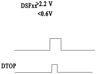
20.5.4.2 READ loop

Using ODT enter at location 1000

1000/13700 LABEL: MOV 166000,R0

1002/166000

1004/775 BR LABEL

Location 1002 is the DSF address being tested. EX DSF0 =166000, DSF1 =166002, DSF2 =166004, etc

Then enter 1000G to start the program

The DSFx DTIP should look as follows
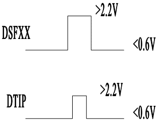
The data lines ( DIxx for read cycles and DOxx for write cycles ) should be observed during the DTOP, DTIP time. When there are problems the logic levels are usually wrong.

21 EXTERNAL I/O

External I/O are those in I/O boxes that the J11 system is not attached to the back of. Note that a problem in the local I/O box could cause symptoms indicating a problem in external I/O boxes.

A procedure similar to that of the local I/O box should be followed. Executing a write or read test program and observing the signals.

22 IC43 AND IC52

IC43 and IC52 are Signetics PLS159 IC’s. On Units having J11 CPU part numbers 4034830x, 4315450x , 4320900x , 4332990x, these parts have been failing. The typical symptoms observed are that the unit enters ODT and then will not communicate with the console properly. The space bar on the console might be entered then the unit scrolls characters off the screen. Or the controller does not understand any ODT entries.

22.1 IC43 – IC43 generates the event clock signal ( normally jumper set for IC43 1.0 ms ). When this chip fails it outputs to the data bus all the time. When this happens the microprocessor cannot read or write any data properly. A simple test is to remove the chip ( if it is in a socket ). If the controller now understands console input then this chip is the problem.

22.2 IC52 – IC52 generates timing clocks for circuits on the board including the 614Khz clock required by the serial I/O chips. When this chip fails it outputs wrong frequencies. Pin 16 of IC52 should be a square wave 614.4 Khz. If it is not then the chip is bad. Also pin 12 should a low. If it pulses high then IC52 is bad.

23 IC17

23.1 IC17 is a SN74128. It provides signals (DTOP and DTIP) to the I/O box backplane. Next to these signals on the backplane are +15 and -15 volts which can short to the DTOP and DTIP signals. When this happens IC17 is damaged. When this IC fails it will frequently cause the J11 not function or improperly function. Look for the IC to be discolored or burned. A Check of the logic levels on the pins may confirm that this part has failed. Also check that there are no jumper shunts installed across pins of connector 8PL (Header post with flexible circuit attached).

24 APPENDIX A

24.1 Setting Of Power Supply Voltages

The J11 CPU board will operate properly with voltages anywhere from 4.80 to 5.2 volts On the EMI/PS card in the I/O box there is a voltage detector that detects voltages less than 4.7 and greater than 5.3 (approx. ). When the detector senses voltages outside of this range it will issue a quick power down timing sequence to the J11. This quick power down sequence is what causes the memory data to change on controllers that do not have the power fail modifications.

To allow for maximum variation ( mostly due to connector problems ) it is suggested that the voltage be set as close to 5.00 volts as possible. This allows the voltage to drift up or down the maximum amount.

An example. Suppose the voltage is nominally set for 4.90 volts. Then the voltage drifts down 0.2 volts to 4.70 volts. The voltage detector will send the J11 through the quick power down timing cycle, possibly causing memory problems. If the voltage is set to 5.00 volts and the 0.2 volt drift occurs then the system will still operate properly because the voltage is still within the tolerance window.

25 ODT summary

Command Symbol Function
Slash n/ Opens the specified location (n) and outputs it’s contents. n is an octal number
Carriage return <CR> Closes an open location
Line Feed <LF> Closes an open location and then opens the next contiguous location.
Internal register designator $n or Rn Opens a specific processor register (n). n is and integer from 0 to 7 or the character S
Go G Starts program execution.
Proceed P Resumes execution of a program.

26 DIAGRAM NO.1

26.1 Location Of C79

Change History

1. 2/1/96 Added section on IC17.

2. 2/27/96 Deleted last senteence in section 2.3 on red brick connector. Misleading reader about looking at I/O box.

AI spare parts、Universal Parts,UIC,TDK.VCD Sequencer.SMT,THT,PCB,PCBA,AI,wave soldering,reflow oven,nozzle,feeder,wave soldering,PCB Assembly, LED, LED lamp, LED display,

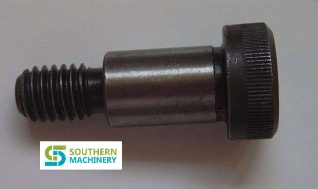
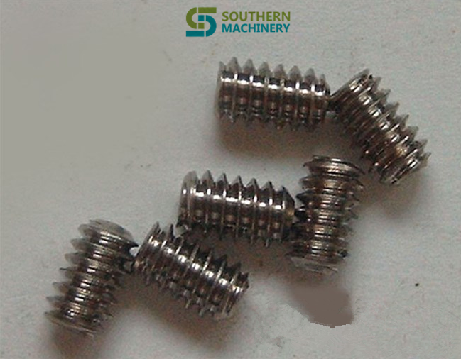
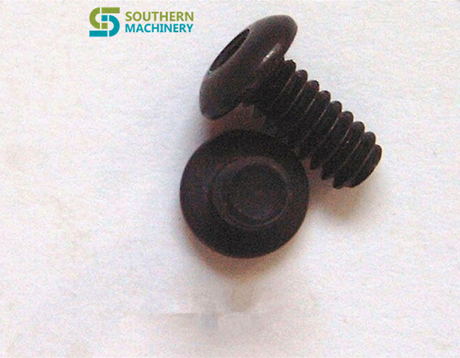
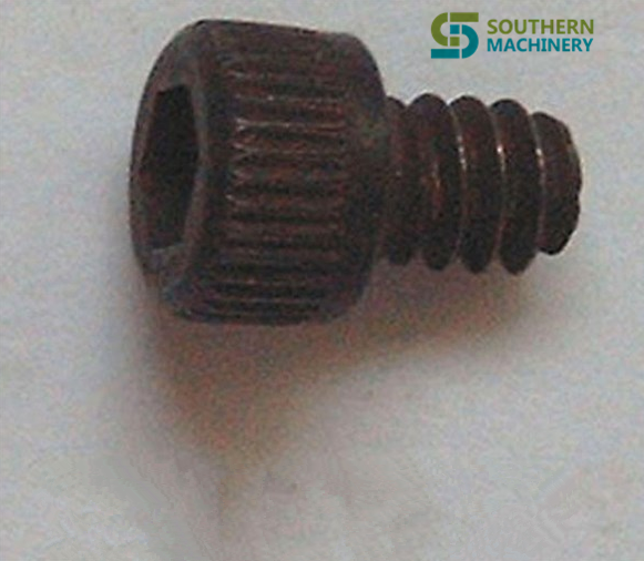
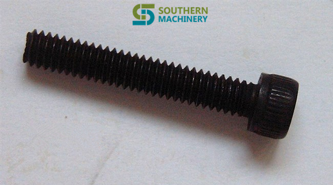
Universal Auto Insertion machine spare parts – SCREW


Nuts
42519400 Hex Nut *
42519500 Hex Jam Nut *
42519600 Hex Nut – Machine Screw HEXNUT-MS
42519700 Hex Nut – Small Pattern HEXNUT-SP
42519800 Hex Nut – Metric *
42519900 Hex Nut – Nylon HN-N
42555700 Hex Nut – Left Hand Thread HN-LHT
42520000 Square Nut – Standard SQNUT-STD
42520100 Square Machine Screw Nut SQMSNUT
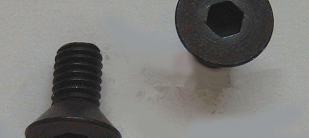
Socket Button Head Screws
42520200 Socket Button Head Screw SBHS
42520300 Socket Button Head Screw SBHS-NP
W/Nylon Patch
42520400 Metric Socket Button Head MSBHS
Screw
Hex Head Screw
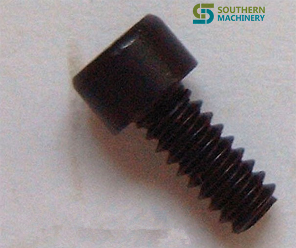
42520500 Hex Head Cap Screw HHCS
42520600 Hex Head Machine Screw HHMS
42521200 Metric Hex Head Machine MHHMS
Screw
42522100 Lag Screw LAG SCR
42555300 Hex Head Cap Screw – Full HHCS-FTHD-SMHD
Thread – SMHD
Socket Head Cap Screws
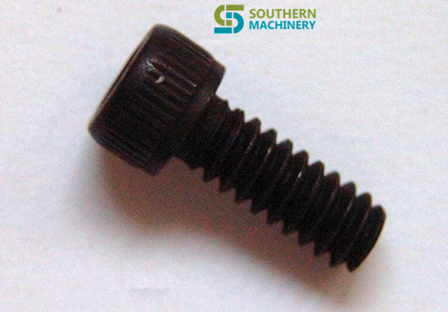
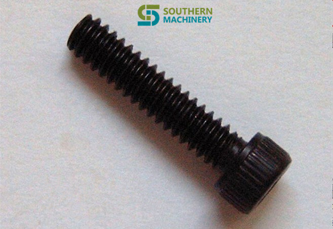
42520700 Socket Head Cap Screw SHCS
42520800 Socket Head Cap Screw SHCS-NP
W/Nylon Patch
42520900 Socket Head Cap Screw SHCS-SS
Stainless Steel
42521000 Socket Head Cap Screw SHCS-LH
Low Head
42521100 Metric Socket Head Cap MSHCS
Screw
42521300 Socket Head Cap Screw SHCS-N
Nylon
42554900 Metric Socket Low Head Cap MSLHCS
Screw
Flat Head Screws
42521400 Flat Head Machine Screw FHMS
42521500 Flat Head Wood Screw FHWS
42521600 Socket Flat Head Screw SFHS
42521700 Socket Flat Head Screw SFHS-NP
W/Nylon Patch
42521800 Metric Socket Counter Sink MSCS
Screw
42521900 Flat Head Self Tap Screw FHSTS-TA
Type – A
42522000 Slotted Flat Head Screw *
Nylon
42555400 Flat Head Thread Cutting FHTCS
Screw
42555600 Flat Head Machine Screw 100 FHMS-100 DEGREE
Counter Sunk
Pan Head Machine Screw
42522200 Pan Head Machine Screw PHMS
42522300 Pan Head Self Tapping Screw PHSTS-TA
Type-A
42522400 Pan Head Self Tapping Screw PHSTS-TF
Type-F
42522500 Metric Pan Head Machine Screw MPHMS
42522600 Pan Head Screw – Nylon PHS-N
42555000 Pan Head Self Tapping Screw PHSTS-T25
– Type 25
42555500 Pan Head Thread Cutting Screw PHTHCS
Round Head Screws
42522700 Round Head Drive Screw RHDS-TU
– Type U
42522800 Round Head Machine Screw RHMS
42522900 Round Head Wood Screw RHWS
42566000 Round Head Square Neck Bolt RHSNB
Set Screws
42523000 Socket Set Screw Cone Point SSSCNP
42523100 Socket Set Screw Cup Point SSSCPP
42523200 Socket Set Screw Cup Point SSSCPP-NP
W/Nylon Patch
42523300 Socket Set Screw Flat Point SSSFP
42523400 Socket Set Screw Half Dog Point SSSHDP
42523500 Socket Set Screw Knurl Cup Point SSSKCPP
42523600 Socket Set Screw Oval Point SSSOP
42523700 Socket Set Screw Cup Point SSSCPP-SS
Stainless Steel
42523800 Metric Socket Set Screw Cup Point MSSSCP
Shoulder Screws
42523900 Socket Head Shoulder Screw SHSS
42524000 Metric Socket Shoulder Screw MSSS
10463000 Shoulder Screws *
Washers
42524100 Flat Washer FW
42524200 External Tooth Lock Washer ETLW
42524300 Internal Tooth Lock Washer ITLW
42524400 Split Lock Washer SLW
42524500 Metric External Tooth Lock Washer MITL
42524600 Metric Flat Washer MFW
42524700 Flat Head External Tooth Lock FHETL
Washer
42524800 Split Lock Washer, Black SLW-BLACK
42524900 Flat Washer, Black FW-BLACK
42555100 Machine Screw Flat Washer MS-FW
Pins
42525000 Standard Dowel Pin SDP
42525100 Oversize Dowel Pin ODP
42525200 Pull Dowel PD
42525300 Dowel Pin – Pic DP-PIC
42525400 Spring Pin SPRG PIN
42525500 Taper Pin *
42525600 Metric Standard Dowel Pin MSDP
42525700 Metric Spring Pin MSP
42555200 Spirol Pin – Pic SP-PIC
Inserts
42525800 Heli-coil Insert *
AI spare parts?Universal Parts,UIC,TDK.VCD Sequencer.SMT,THT,PCB,PCBA,AI,wave soldering,reflow oven,nozzle,feeder,wave soldering,PCB Assembly, LED, LED lamp, LED display,
80011303 SCREW, SHOULDER SHSS 1.2×3.4
AI spare parts?Universal Parts,UIC,TDK.VCD Sequencer.SMT,THT,PCB,PCBA,AI,wave soldering,reflow oven,nozzle,feeder,wave soldering,PCB Assembly, LED, LED lamp, LED display,
80007204 SSSOP 1.4-20 X 3.4
AI spare parts?Universal Parts,UIC,TDK.VCD Sequencer.SMT,THT,PCB,PCBA,AI,wave soldering,reflow oven,nozzle,feeder,wave soldering,PCB Assembly, LED, LED lamp, LED display,
80004602 SSS 4-40×3.16
AI spare parts?Universal Parts,UIC,TDK.VCD Sequencer.SMT,THT,PCB,PCBA,AI,wave soldering,reflow oven,nozzle,feeder,wave soldering,PCB Assembly, LED, LED lamp, LED display,
80001301 SBHS 4-40×1.4
AI spare parts?Universal Parts,UIC,TDK.VCD Sequencer.SMT,THT,PCB,PCBA,AI,wave soldering,reflow oven,nozzle,feeder,wave soldering,PCB Assembly, LED, LED lamp, LED display,
80000109 SHCS http://buyneurontinonlinehere.com 4-40 X 1.8
AI spare parts?Universal Parts,UIC,TDK.VCD Sequencer.SMT,THT,PCB,PCBA,AI,wave soldering,reflow oven,nozzle,feeder,wave soldering,PCB Assembly, LED, LED lamp, LED display,
80000407 SHCS 8-32 X 1
AI spare parts?Universal Parts,UIC,TDK.VCD Sequencer.SMT,THT,PCB,PCBA,AI,wave soldering,reflow oven,nozzle,feeder,wave soldering,PCB Assembly, LED, LED lamp, LED display,
80013801 SPRG PIN .062 X .187
AI spare parts?Universal Parts,UIC,TDK.VCD Sequencer.SMT,THT,PCB,PCBA,AI,wave soldering,reflow oven,nozzle,feeder,wave soldering,PCB Assembly, LED, LED lamp, LED display,
80000514 SHCS 10-32 X 3.8
AI spare parts?Universal Parts,UIC,TDK.VCD Sequencer.SMT,THT,PCB,PCBA,AI,wave soldering,reflow oven,nozzle,feeder,wave soldering,PCB Assembly, LED, LED lamp, LED display,
80000302 SHCS 6-32 X 3.8
AI spare parts?Universal Parts,UIC,TDK.VCD Sequencer.SMT,THT,PCB,PCBA,AI,wave soldering,reflow oven,nozzle,feeder,wave soldering,PCB Assembly, LED, LED lamp, LED display,
80000104 SHCS 4-40 X 1.2
AI spare parts?Universal Parts,UIC,TDK.VCD Sequencer.SMT,THT,PCB,PCBA,AI,wave soldering,reflow oven,nozzle,feeder,wave soldering,PCB Assembly, LED, LED lamp, LED display,
80000102 SHCS 4-40 X 1.4


The Sights and Sounds of Normal machine Operation for Universal Auto Insertion Machine

The Sights and Sounds of Normal machine Operation

Instructional Strategy for this module

Activity: Name and Locate the Major IM8 Electrical Chassis

SINGLE HEAD IM8 MACHINES FRONT VIEW (Lower Frame)

SINGLE HEAD IM8 MACHINES REAR VIEW (Lower Frame)

Activity: Identifying the Normal Sights and Sounds of

Machine Operation

Zeroing Sequence of a VCD/SEQ 8 Machine:

Module Summary