AI spare parts、Universal Parts,UIC,TDK.VCD Sequencer.SMT,THT,PCB,PCBA,AI,wave soldering,reflow oven,nozzle,feeder,wave soldering,PCB Assembly, LED, LED lamp, LED display

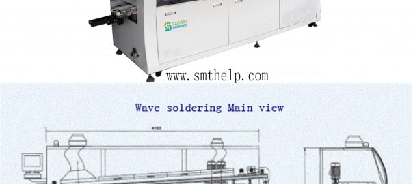
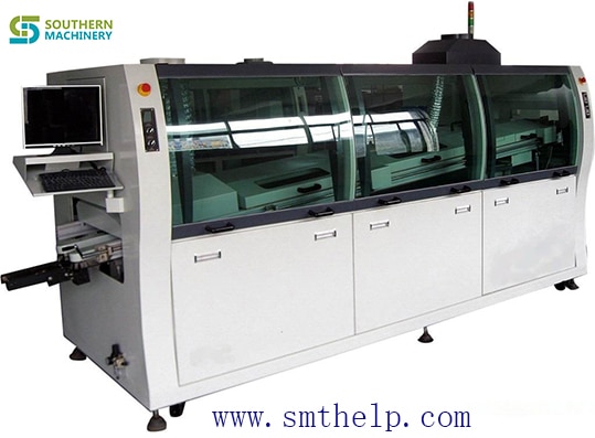
S-ws250 Wave soldering machine for electronic manufacturing PCBA

Lead-free or Tin-lead Through-hole Soldering

adjustable dual waves permit lead-free or tin/lead processing of through-hole and SMD boards to a maximum width of 250 mm

As PCBs are loaded onto the adjustable titanium finger conveyor, they are automatically prepped by an adjustable internal spray fluxing system which houses a precision spray nozzle assembly mounted to a reciprocating Y-axis drive mechanism to ensure even and accurate application of flux.

Run as Dual or Single Wave

Solder processing temperature is settable to a lead-free compatible 300°C. The system includes an economical low-volume 200 kg (550 lbs. Approximate weight for lead free solder) capacity solder pot with an easy-handling roll-out feature. A built-in alarm signals when solder level is at the refill point.

Forced Hot Air Convection Pre-Heat

The preheat stage takes place in a 600 mm (23.6″) glass-covered chamber where boards are heat-bathed by energy-saving forced hot air convection, as opposed to power-consuming, uneven IR heat.

AI spare parts、Universal Parts,UIC,TDK.VCD Sequencer.SMT,THT,PCB,PCBA,AI,wave soldering,reflow oven,nozzle,feeder,wave soldering,PCB Assembly, LED, LED lamp, LED display


Automatic spray fluxer produces uniform fine spray coverage of underside of each incoming board. Integrated cooling zone provides rapid cooling for processed boards prior to exiting the conveyor.
Energy-conserving 600 mm (23.6”) forced hot air convection preheater safely preps boards for higher temperatures of lead-free or tin-lead soldering while ensuring that fluxes are properly activated. Process area—where dual waves are generated by titanium alloy wave nozzles.
Preheat area remains enclosed under glass during processing, preventing escape of hot air. With front panel removed, dual solder pumps (top) and solder pot below are exposed. Electrical panel is accessed by removing cabinet door on right side.
Cooling fans apply focused below-board heat to quickly lower temperatures of processed boards. Titanium-alloy wave nozzle and components resist corrosion. Finger conveyors are automatically cleaned prior to loading of each board.
Titanium finger conveyor is hand-crank adjustable to boards of up to 350 mm width. Titanium finger conveyor is hand-crank adjustable to boards up to 350 mm width. Fingers are self cleaning.
Built-in flux fume exhaust hood and filter. Flux vapors are extracted through a built-in fume hood and filter, and out of the system through an exhaust flange on the top of the unit. The filter is easily removable for cleaning. A tote case containing all hand tools necessary for maintenance, repair or disassembly
AI spare parts、Universal Parts,UIC,TDK.VCD Sequencer.SMT,THT,PCB,PCBA,AI,wave soldering,reflow oven,nozzle,feeder,wave soldering,PCB Assembly, LED, LED lamp, LED display,

SMT Pick And Place machine Spare parts

We can supply smt machine parts, smt spare parts, replacement parts for pick and place machine, Brands including FUJI, SIEMENS, PANASONIC, JUKI, YAMAHA, , etc.


Part of product list: 

Compatible for

Part name

Part No.

Usage

fuji NXT H01

H01 Filter (with plastic BKT)

AA1FZ01

Consumable parts

fuji NXT H12

H12 Filter (with plastic BKT)

AA19H02

Consumable parts

fuji NXT H01

H01 smt filter

XH00560

Consumable parts

fuji

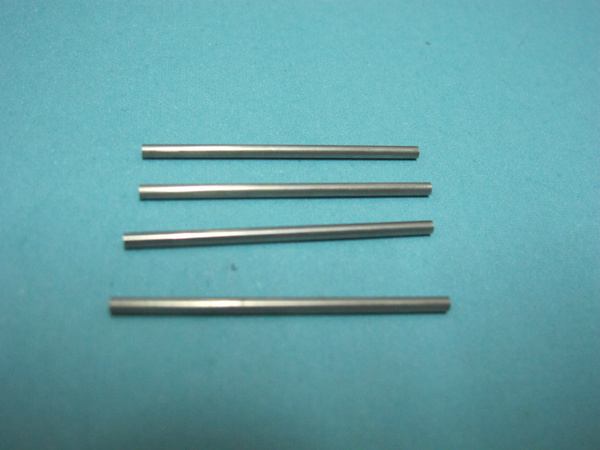
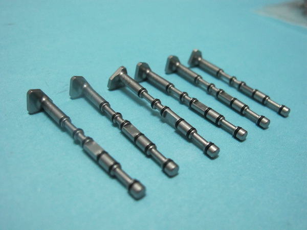
smt pin thick pin

ADCQK8010

replacement parts

fuji

smt pin thin pin

ADCQK8010

replacement parts

fuji XP243

XP243 U axis PULLEY

AGFTR8220

replacement parts

fuji XP243

XP243 U axis PULLEY

AGFTR8230

replacement parts

fuji

fuji sliding block and thimble

O0186

replacement parts

fuji CP6

CP6 HOLDER

AWPH3110

replacement parts

fuji CP43

CP43 CLUTCH

MPH0501

replacement parts

fuji QP242

QP242 Filter

H3022T

Consumable parts

fuji CP41

CP41 press button

O0191

replacement parts

fuji IP3

IP3 Filter

H30215

Consumable parts

fuji CP6

cylinder

WPA5150

Consumable parts

fuji CP7 CP8

smt filter

DCPH3780

Consumable parts


AI spare parts、Universal Parts,UIC,TDK.VCD Sequencer.SMT,THT,PCB,PCBA,AI,wave soldering,reflow oven,nozzle,feeder,wave soldering,PCB Assembly, LED, LED lamp, LED display,
H10212
angela@smthelp.net

AI spare parts、Universal Parts,UIC,TDK.VCD Sequencer.SMT,THT,PCB,PCBA,AI,wave soldering,reflow oven,nozzle,feeder,wave soldering,PCB Assembly, LED, LED lamp, LED display,
H13362
angela@smthelp.net

AI spare parts、Universal Parts,UIC,TDK.VCD Sequencer.SMT,THT,PCB,PCBA,AI,wave soldering,reflow oven,nozzle,feeder,wave soldering,PCB Assembly, LED, LED lamp, LED display,
H30105
angela@smthelp.net

AI spare parts、Universal Parts,UIC,TDK.VCD Sequencer.SMT,THT,PCB,PCBA,AI,wave soldering,reflow oven,nozzle,feeder,wave soldering,PCB Assembly, LED, LED lamp, LED display,
H42693
angela@smthelp.net

AI spare parts、Universal Parts,UIC,TDK.VCD Sequencer.SMT,THT,PCB,PCBA,AI,wave soldering,reflow oven,nozzle,feeder,wave soldering,PCB Assembly, LED, LED lamp, LED display,
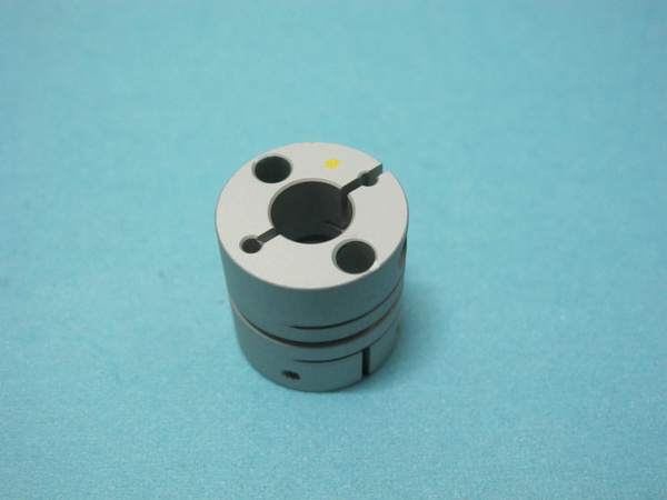
K1006L COUPLING
angela@smthelpl.com

AI spare parts、Universal Parts,UIC,TDK.VCD Sequencer.SMT,THT,PCB,PCBA,AI,wave soldering,reflow oven,nozzle,feeder,wave soldering,PCB Assembly, LED, LED lamp, LED display,
H3022T
angela@smthelp.net

AI spare parts、Universal Parts,UIC,TDK.VCD Sequencer.SMT,THT,PCB,PCBA,AI,wave soldering,reflow oven,nozzle,feeder,wave soldering,PCB Assembly, LED, LED lamp, LED display,
H3022L
angela@smthelp.net

AI spare parts、Universal Parts,UIC,TDK.VCD Sequencer.SMT,THT,PCB,PCBA,AI,wave soldering,reflow oven,nozzle,feeder,wave soldering,PCB Assembly, LED, LED lamp, LED display,
H2002Y
angela@smthelp.net

AI spare parts、Universal Parts,UIC,TDK.VCD Sequencer.SMT,THT,PCB,PCBA,AI,wave soldering,reflow oven,nozzle,feeder,wave soldering,PCB Assembly, LED, LED lamp, LED display,
GFPH2540
angela@smthelp.net

AI spare parts、Universal Parts,UIC,TDK.VCD Sequencer.SMT,THT,PCB,PCBA,AI,wave soldering,reflow oven,nozzle,feeder,wave soldering,PCB Assembly, LED, LED lamp, LED display,
GFPN1160
angela@smthelp.net

AI spare parts、Universal Parts,UIC,TDK.VCD Sequencer.SMT,THT,PCB,PCBA,AI,wave soldering,reflow oven,nozzle,feeder,wave soldering,PCB Assembly, LED, LED lamp, LED display,
H1124D
angela@smthelp.net

AI spare parts、Universal Parts,UIC,TDK.VCD Sequencer.SMT,THT,PCB,PCBA,AI,wave soldering,reflow oven,nozzle,feeder,wave soldering,PCB Assembly, LED, LED lamp, LED display,
A10397
angela@smthelp.net

AI spare parts、Universal Parts,UIC,TDK.VCD Sequencer.SMT,THT,PCB,PCBA,AI,wave soldering,reflow oven,nozzle,feeder,wave soldering,PCB Assembly, LED, LED lamp, LED display,
2MGKCF001600
angela@smthelp.net
XS01802=XS03693 SPOOL NXT 原装全新..

Xi highlights poverty reduction, int’l role in New Year speech:SMT is looking forward to solutions from China

Let’s grow our ‘circle of friends’ .

http://www.chinadaily.com.cn/china/2015-12/31/content_22890743.htm

BEIJING – President Xi Jinping highlighted poverty reduction and China’s international role in his New Year speech Thursday.

In an address transmitted live by state broadcasters, Xi called for confidence and hard work for a good beginning in the home stretch of building a “moderately prosperous society in all respects.”

Xi said that a meeting of the Communist Party of China (CPC) in late October set out a promising and encouraging blueprint for development over the next five years.

Xi noted that lifting tens of millions of rural people out of poverty was his top concern, and called for joint efforts to achieve this goal.

“We should care for all people facing difficulties, making them feel warm from the bottom of their hearts,” Xi said.

It is the third New Year speech Xi has given since 2013.

PAINS AND GAINS

Xi extended his New Year wishes to Chinese people of all ethnic groups, compatriots in Hong Kong and Macao, compatriots in Taiwan and overseas Chinese, as well as friends from other countries and regions.

“In 2015, Chinese people gave a lot, and we received a lot too,” Xi said, citing the fact that the country’s economic growth continues to be among the fastest in the world, reforms are in full swing and there has been deepened judicial reform.

The “three stricts and three earnests” campaign and anti-corruption fight have also been improving the country’s political environment.

Xi recalled the large-scale commemoration for the 70th anniversary of victory in the Chinese People’s War of Resistance Against Japanese Aggression and in the World Anti-Fascist War. During the event, Xi announced China will cut troops by 300,000.

“Our commemorative activities and the grand military parade showcased the truth that justice will prevail, peace will prevail and the people will prevail,” Xi said.

Xi noted that his meeting with Ma Ying-jeou in Singapore in November and their handshake, the first between leaders of the two sides of the Taiwan Strait in 66 years, reflected the common wish of compatriots from both sides for the peaceful development of cross-Strait relations.

The president cited more milestone moments, including Beijing winning the bid to host the 24th Winter Olympics, the RMB’s inclusion into the currency basket of the Special Drawing Rights of the International Monetary Fund, China’s first homemade large passenger aircraft C919 rolling off the assembly line, Tianhe-2 supercomputer remaining the world’s most powerful system for the sixth consecutive time, the country’s first space telescope to search for signals of dark matter sent into space and Tu Youyou winning the Nobel Prize in Physiology or Medicine.

“All these show us that, as long as we persevere, dreams will come true,” Xi said.

“This year, we had joys, but we also had sorrows,” Xi said, recalling cruise ship Eastern Star capsizing, catastrophic fires and explosions at a chemical warehouse in Tianjin and the Shenzhen landslide.

“These accidents led to many lives lost, and it’s also deeply harrowing that our compatriots were cruelly killed by terrorists,” Xi said. “We mourn them, and hope that the deceased rest in peace and the living are safe and healthy.”

Recognizing that people still have difficulties and troubles, Xi vowed that the Party and the government will continue to make concrete efforts to protect people’s lives and property, improve their livelihoods and ensure their health.

INT’L PLAYER

China must not be absent from international affairs, as the world is looking forward to voices and answers from China, Xi said.

“The world is so big, the challenges so complicated, ” he said.

“For those people torn by hardship and war, we need to offer not only sympathy and compassion, but also responsibility and action,” Xi said.

“China will always welcome the world with an open embrace, and we will also extend our hand to those in difficulty as best as we can, and our ‘circle of friends’ will grow,” Xi said, borrowing a term from the popular messaging app WeChat.

Throughout 2015, Xi said, China’s leaders have taken active part in international conferences and diplomatic activity, bringing substantial progresses in the “Belt and Road Initiative,” while contributing to the United Nations 2030 agenda for sustainable development and the global fight against climate change.

He said, “We have only one earth, one home for the peoples of all nations.”

Xi expressed his earnest hope that the international community could work together for peace, in a spirit of cooperation. “By turning antagonism to synergy, hostility to friendship, together we will forge a community of shared destiny for all humankind,” said the president.

Bearing press fit calculation

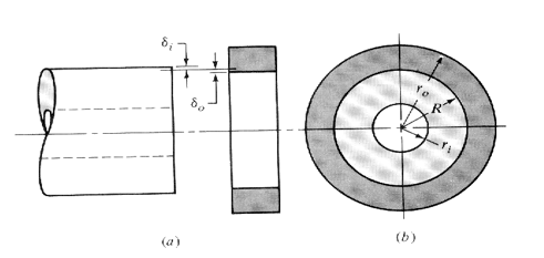
This calculates the delfection of the outer race of a bearing when it is pressed into a housing.

These equations are from Shigley and Mischke “Mechanical Engineering Design” Fifth Ediion p.62-63

Bearing

Housing

Modulus of Elasticity of Inner component (Ei)

30000000

Modulus of Elasticity of Outer component (Eo)

10300000

Inner Radius of Inner Component (land radius)(ri)

0.1705

Outer Radius of Outer Component (ro)

0.3

Poisson’s Ratio of Inner Component (vi)

0.292

Poission’s Ratio of Outer Component (vo)

0.334

Radius at Press (interface) (R)

0.1875

Radial Press (d)

0.0003

Results

Resulting Pressure (p)

2599.55178212877

Increase in Housing Outer Radius (delta ro)

0.000123796616002366

Decrease in Bearing Inner Radius of OD (delta ri)

0.000176203383997634

Assumptions:

Both members have the same length.

Cross sections are uniform.

Radial interference is constant around the circumference.

AI spare parts、Universal Parts,UIC,TDK.VCD Sequencer.SMT,THT,PCB,PCBA,AI,wave soldering,reflow oven,nozzle,feeder,wave soldering,PCB Assembly, LED, LED lamp, LED display,

Acceptability for Electronic Assemblies :Soldering Acceptability Requirements

Acceptability for Electronic Assemblies :Soldering Acceptability Requirements


Target-Class1,2,3
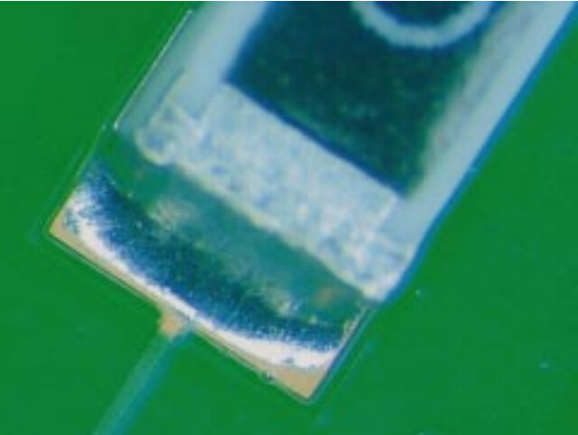
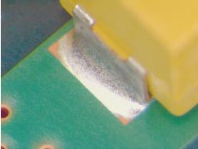
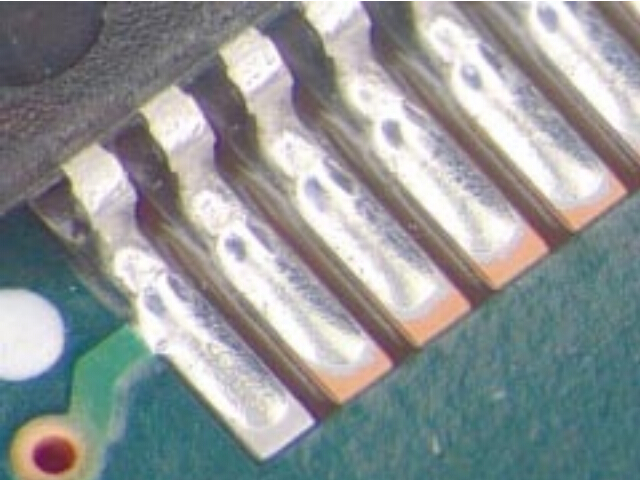
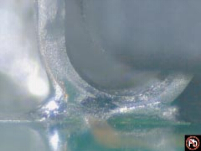
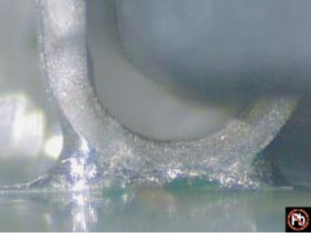
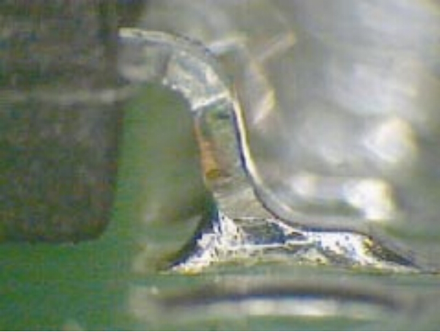
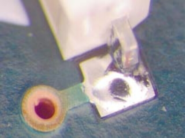
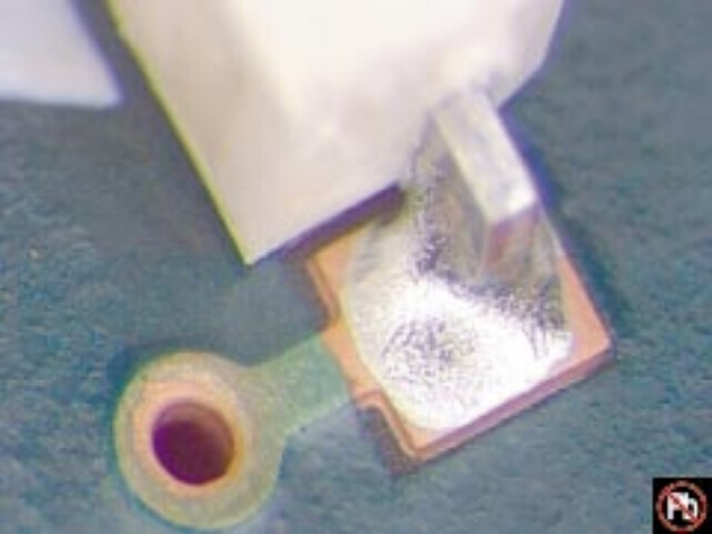
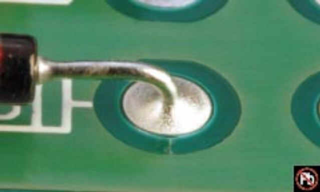
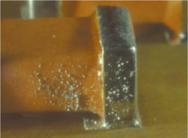
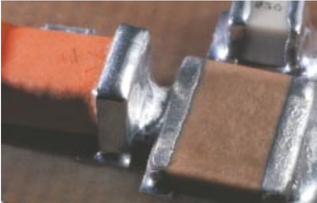
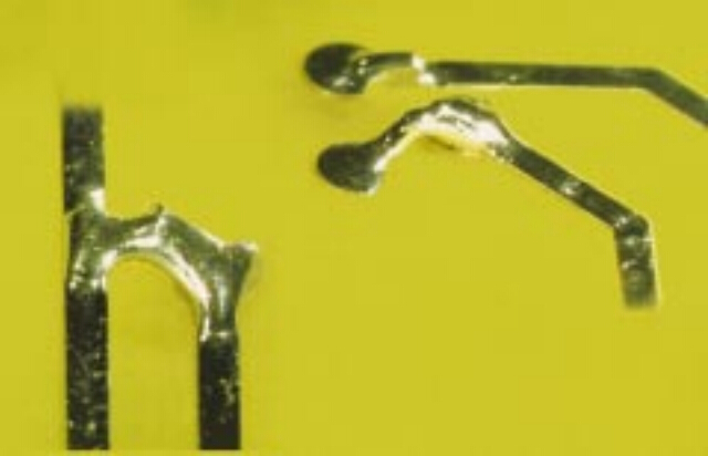
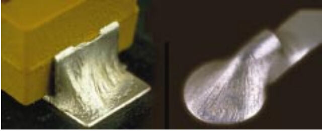
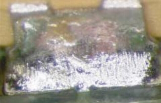
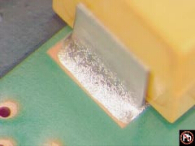
.Solder fillet appears generally smooth and exhibits good wetting of the solder to the parts being joined.
.Outline of the parts is easily determined.
.Solder at the part being joined creates a feathered edge.
.Fillet is concave in shape.


p1s1

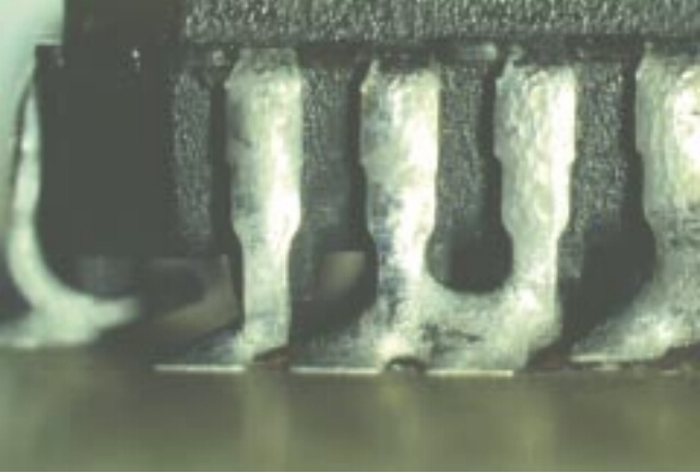
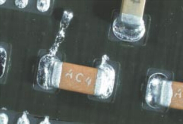
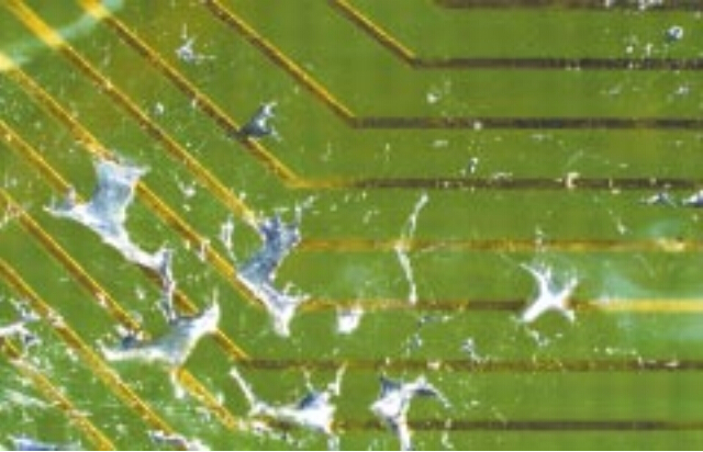
See pic for examples of soldering anomalies.

Acceptable-Class1,2,3
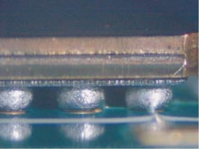
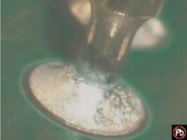
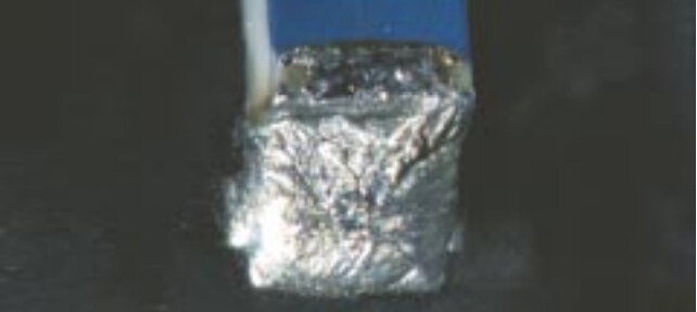
.There are materials and processes,e.g.,lead free alloys and slow cooling with large mass PCBs, that may produce dull
matte,gray,or grainy appearing solders that are normal for the material or process involved.These solder connections
are acceptable.
.The solder connection wetting angle (solder to component and solder to PCB termination do not exceed 90°(Figure).
.As an exception,the solder connection to a termination may exhibit a wetting angle exceeding 90°(Figure)when it is 

created by the solder contour extending over the edge of the solder able termination area or solder resist.


p1s2


Figures below illustrate acceptable solder connections with various solder alloys and process conditions.

p2s1 p2s2

SnPb Solder; No Clean Process                                     SnAgCu Solder;No Clean Process

p2s3 p2s4

    SnPb Solder;Water Soluble Flux                                 SnAgCu Solder;Water Soluble Flux

p2s5 p2s6

   SnPb Solder; Water Soluble Flux                                 SnAgCu Solder;Water Soluble Flux

p3s1 p3s2

     SnAgCu Solder;No Clean Process,N2 Reflow                 SnAgCu Solder,No Clean Process;Air Reflow

p3s3 p3s4

      SnPb Solder;No Clean Process                                  SnAgCu Solder;No Clean Process

p3s5 p3s6

     SnPb Solder;No Clean Process                                   SnAgCu Solder;No Clean Process

p4s1 p4s2

                        SnPb Solder                                                      SnAgCu Solder

p4s3 p4s4

                     SnPb Solder                                                           SnAgCu Solder

p4s5 p4s6

         SnPb Solder ; OSP Finish                                                       SnAgCu Solder; OSP Finish

p5s1 p5s2

                     SnAg CuSolder                                                      SnAg CuSolder

p5s3 p5s4

                 SnAgCu  Solder                                                         SnAgCu Solder


       Soldering Anomalies-Exposed Basis Metal

Exposed basis metal on component leads,conductors or land surfaces from nicks,scratches,or other conditions cannot exceed
there quirements of 7.1.2.3 for leads and 10.2.9.1 for conductors and      lands.
Component leads,sides of land patterns,conductors,and use of liquid photo image able solder resist,can have exposed basis
metal per original designs.
Some printed circuit board and conductor finishes have different wetting characteristics and may exhibit solder wetting only to
specific areas. Exposed basis metal or surface finishes should be considered normal under these circumstances,provided the
achieved wetting characteristics of the solder connection areas are acceptable.


Acceptable-Class 1,2,3
.Exposed basis metal on:
.Vertical conductor edges.
.Cut ends of component leads or wires.
.Organic Solderability Preservative (OSP) coated lands.
.Exposed surface finishes that are not part of the required solder fillet  area.

p6s1 p7s1


Acceptable-Class 1

Process Indicator-Class 2,3

.Exposed basis metal on component leads,conductors or land surfaces from nicks or scratches provided conditions

do not exceed the requirements of7.1.2.3 for leads and 10.2.9.1 for conductors and lands.

p7s2


 Soldering Anomalies-Pin Holes/Blow Holes


Acceptable-Class1
ProcessIndicator-Class2,3

.Blowholes (Figures 1,2),pinholes (Figure 3),voids (Figures 4,5),etc.,providing the solder connection meets all other requirements.


p8s1 p8s2                           

                          1                                                                                2                                                                        

p8s3 p8s4

                             3                                                                                 4

 p8s5                     

                                  5

Defect-Class 2,3

Solder connections where pin holes,blowholes,voids,etc.
reduce the connections below minimum requirements(not shown).


Soldering Anomalies-Reflow of Solder Paste

 Defect-Class1,2,3
.Incomplete reflow of solder paste.


p9s1

 p9s2


Soldering Anomalies-Nonwetting

IPC-T-50 defines nonwetting as the inability of molten solder to form a metallic bond with the basis metal.In this Standard,that
includes surface finishes.

Defect-Class 1,2,3
.Solder has not wetted to the land or termination where solder is required.
.Solder coverage does not meet requirements for this termination type.

p10s1

p10s2

p10s3

p10s4

p10s5


Soldering Anomalies-Dewetting

Defect-Class 1,2,3
.Evidence of dewetting that causes the solder connection to not meet the SMT and thru-hole solder fillet requirements.


p11s1

p11s2

p11s3


                          Soldering Anomalies-Excess Solder-Solder Balls/Solder Fines

Solder balls are spheres of solder that remain after the soldering process.Solder fines are typically small balls of the original 

solder paste metal screen size that have splattered around the connection during there flow process.


Target-Class 1,2, 3
.No evidence of solder balls on the printed wiring assembly.

p12s1

Acceptable-Class 1,2,3
.Solder balls are entrapped/encapsulated and do not violate minimum electrical clearance.
 Note:Entrapped/encapsulated/attached is intended to mean that normal service environment of the product will not cause a solder ball to become dislodged.

p12s2


Defect- Class 1,2,3
.Solder balls violate minimum electrical clearance.
.Solder balls are not entrapped in no-clean residue or encapsulated with conformal coating,

or not attached(soldered)to a metal surface.

p13s1

p13s2

p13s3

p13s4


Soldering Anomalies-Excess Solder-Bridging


Defect-Class 1,2,3
.A solder connection across conductors that should not be joined.
.Solder has bridged to adjacent noncommon conductoror component.

p14s1

p14s2

p14s3

p14s4


Soldering Anomalies-Excess Solder-Solder Webbing/Splashes

Defect-Class 1,2,3
.Solder splashes/webbing.


p15s1

p15s2


Soldering Anomalies-Disturbed Solder

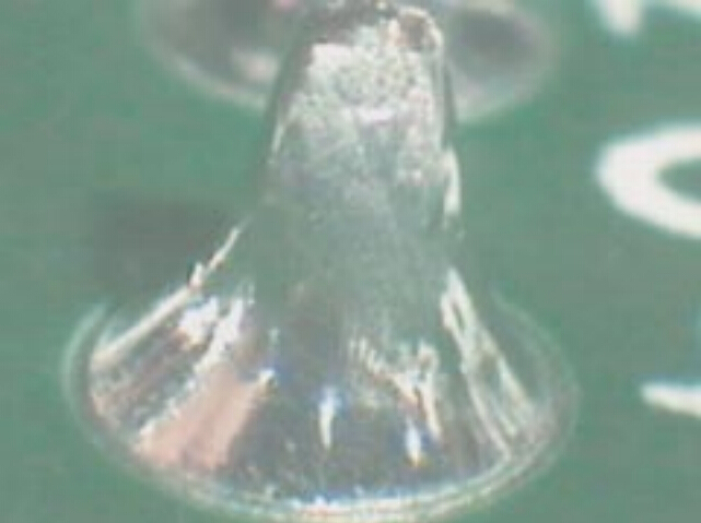
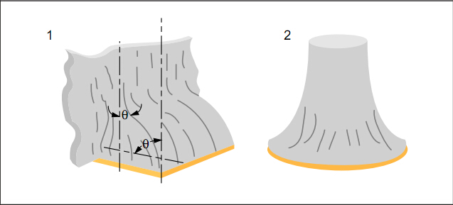
Surface appearance with cooling lines as shown in Acceptable pic is more likely to occur in lead free alloys and is not a disturbed solder condition.

p16s1


Defect-Class 1,2,3
Characterized by stress lines from movement in the connection (SnPb alloy).

p16s2

p16s3

p16s4

p16s5


Soldering Anomalies-Fractured Solder


Defect-Class 1,2,3
Fractured or cracked solder.


p17s1

p17s2


Soldering Anomalies-Solder Projections

Defect-Class 1,2,3
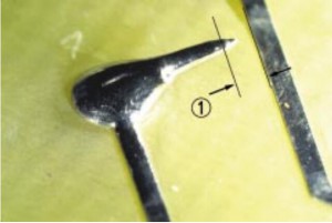
.Solder projection,figure 1,violates assembly maximum
height requirements or lead protrusion requirements.
.Projection,figure 2,violates minimum electrical clearance(1).


p18s1 p18s2

                       1                                                              2


p18s3


Soldering Anomalies-Lead Free Fillet Lift

Acceptable-Class 1,2.3
.Fillet lifting-separation of the bottom of the solder and the
top of the land(primary side of plated-through hold connection).

Process Indicator-Class 2
Defect-Class3

.Fillet lifting-separation of the bottom of the solder and the top of the land(secondary side of plated-through hold connection)(not shown).
Defect-Class 1,2,3
.Fillet lifting damages the land attachment.

p19s1


Soldering Anomalies-Hot Tear/Shrink Hole

Acceptable-Class1,2,3
.For connections made with lead free alloys:
.The bottom of the tear is visible.
.The tear or shrink hole does not contact the lead,land or
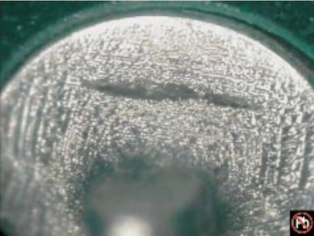
barrel wall.


Defect-Class 1,2,3
.Shrink holes or hot tear in connections made with SnPb  
solder alloys:

.For connections made with lead free alloys:
.The bottom of the shrink hole or hot tear is not visible.
.The tear or shrink hole contacts the lead or land.

p20s1

                                   end

Debugger reference manual for SMT machine Radysis Motion Controler

UBUG Users Guide ( Debugger reference manual )

for Radysis Motion Controler


 The
UBUG monitor is a stand alone software package designed to allow
evaluation and debugging of the UIMC 68EC030 based motion controller
PCB. It has the capability to load and execute user code and includes
an assembler/disassembler designed for quick program patchwork. The
monitor operates in a user interactive command driven mode signified by
the UIC> prompt. The command line entered after this prompt
determines which operation is performed.


         UBUG MONITOR


TABLE OF CONTENTS


1. GENERAL INFORMATION  

         1.1  Description of UBUG…………………..  3


2. THE UBUG COMMAND SET

         2.1  Introduction…………………………    3

         2.2  Auto Null (an)………………………    4

         2.3  Assembler/Disassembler (as) …………..  4

         2.4  Block of Memory Fill (bf)……………..  6

         2.5  Block of Memory Move (bm)……………..  6

         2.6  Break Point (br)……………………..    6

         2.7  Block Search (bs)…………………….    7

         2.8  Counter Test (ct)……………….      7

         2.9  DAC16, ADC8 Test (dac16t)…………….  7

         2.10  Data Conversion (dc)………………….  8

         2.11  Go (go)……………………………..    8

         2.12  Help (?/he/help)……………………..    8

         2.13  IO Access (io)………………..      8

         2.14  Load S-Records (lo)…………………..  9

         2.15  Memory Display (md)…………………..  9

         2.16  Memory Modify (mm)……………………  10

         2.17  Memory Test (mt)…………………..    10

         2.18  Register Display (rd)…………………    10

         2.19  Register Modify (rm)………………….  11

         2.20  Symbol Define (sd)……………………  11

         2.21  Test – Diagnostic (test)……………….    11

         2.22  Transparent Mode ™…………………  12

         2.23  Trace (tr)…………………………..    12


3 USING THE ONE-LINE ASSEMBLER/DISASSEMBLER

         3.1  Introduction ……………………….    12

         3.2  Entering and Modifying Source Program ….  12

       
 3.3  Entering a Source Line………………..  13          
 3.4  Entering a Change of Flow Instr ………  14

       
 3.5  Entering Register Lists ………………  15          
 3.6  Entering Floating Point Immediate Data …  16          
 3.7  Entering MMU Instructions …………….  17


1.  GENERAL INFORMATION


1.1  DESCRIPTION OF UBUG

 The
UBUG monitor is a stand alone software package designed to allow
evaluation and debugging of the UIMC 68EC030 based motion controller
PCB. It has the capability to load and execute user code and includes
an assembler/disassembler designed for quick program patchwork. The
monitor operates in a user interactive command driven mode signified by
the UIC> prompt. The command line entered after this prompt
determines which operation is performed.


2.  THE UBUG COMMAND SET


 2.1  INTRODUCTION

 This
section explains the UBUG monitor commands and their associated syntax.
Table 2.1 summarizes the available commands and shows the section where
the command is explained in greater detail.


TABLE 2.1 UBUG MONITOR COMMANDS


Command/Mnemonic

Name

Section

an

Auto Null

2.2

as

Assembler/Disassembler

2.3

bf

Block of Memory Fill

2.4

bm

Block of Memory Move

2.5

br

Breakpoint

2.6

bs

Block of Memory Search

2.7

ct

Counter Test

2.8

dac16t

DAC16, ADC8 Test

2.9

dc

Data Conversion

2.10.

go

Go

2.11

?/he/help

Help

2.12

io

IO Access

2.13

lo

Load S-Records

2.14

md

Memory Display

2.15

mm

Memory Modify

2.16

mt

Memory Test

2.17

rd

Register Display

2.18

rm

Register Modify

2.19

sd

Symbol Define

2.20.

test

Test – Diagnostic

2.21

tm

Transparent Mode

2.22

tr

Trace

2.23


 The command line is composed of:

 <COMMAND IDENTIFIER>: specifies which command (ex. br )

 <SP>:   at least one space

  OPTION LIST: an option may use delimiter(-) with options if non-default
options    are allowed and are being used. (ex.
[<-r>])

  <SP>: at least one space

  ARGUMENTS: any required arguments specified by the command separated
    by commas/spaces as shown in the command
description. (ex. <ADDR,ADDR>)


 where “<>” enclose symbols that are required on the command line
and “[<>]” enclose symbols that are optional on the command
line. Note, in the above examples the -r option was an example of an
optional symbol and that the ADDR fields are requirements on the
command line. The options available with a given command are fully
explained in the section that describes that command. The monitor is
not case sensitive to input from the terminal. All input from the
terminal is converted to lower case before being used internally (except
text following a text delimiter; See TEXT below). The arguments of a
given command are described using the following symbols:


 <EXP>: An expression can be any numerical expression which may
be evaluated using only the arithmetic + and – operators.

 Ex. 1000

    Ex. 1+3


 Note: Numbers may be preceded with a base designator if the default
(hexadecimal) is not desired. These designators are shown below in Table
2.2:


TABLE 2.2 BASE DESIGNATORS

Base

Designator

Hexadecimal

$

Decimal

&

Octal

@

Binary

%


 <ADDR>: Address field is any valid expression. Note: This
address field should not be      confused with the source and
destination addresses required using the        Assembler/Disassembler.


  <COUNT>: Count field is any valid expression preceded by a COUNTDEL (count      delimiter ie. “:”)

 Ex. :100


 <RANGE>: A range of memory locations denoted by either ADDR,ADDR or        ADDR:COUNT.

 Ex. 0,100

    Ex. 0:50


  <TEXT>: An ASCII string of up to 255 characters preceded by a TEXTDEL (text    delimiter i.e.. “;”)

 Ex. ;sample text


  <SIZE>: Can be either:

    byte (8 bit)  ====> -b

    word (16 bit  )  ====> -w

    long (32 bit)  ====> -l

**Note: ====> stands for “is represented by” or “returns”


 <DATA>: Data can be any valid expression.


  <MASK>: A mask may be any expression. After evaluating the
expression 0’s      represent don’t cares. A mask is sometimes
used to qualify


 <DATA>. See section 2.6 for an example of usage.


2.2  AUTO NULL

 an <AXIS>


 The auto null function performs a nulling of the zero offset of the 16bit DAC of the axis specified.


 Examples of use:

 an 1    ( nulls axis one )


2.3   ASSEMBLER/DISASSEMBLER

 as <ADDR>


 The assembler/disassembler is invoked at the address given and
disassembles the object code at that location. Use of the
Assembler/Disassembler is fully described in chapter 3.


2.4   BLOCK OF MEMORY FILL

 bf [<SIZE>] <RANGE> <DATA>


 The block fill command fills the specified range of memory with the
data listed. If the size option is not specified the default size used
is word. If a multiple of the <SIZE> of <DATA> does not
fit evenly in the <RANGE> the command leaves the last partial
word or long word unchanged.

 Examples of use:

         bf 100,110  &10

  bf 100:8    &10

 bf -w 100:8   a

 bf -l 100,110    a000a

**Note: All of these examples perform the same memory fill.

        (ie. $00000100: $000a $000a $000a $000a $000a $000a

 $0000010C: $000a $000a $0000 $0000 $0000 $0000 )


2.5   BLOCK OF MEMORY MOVE

 bm [<SIZE>] <RANGE> <ADDR>


 The block move command allows the user to copy segments of memory to
different locations in memory. The execution of this command does not
destroy the original version unless the location moved to <ADDR>
is within the range <RANGE> of the code being copied. The size
option is only available when range is described as
<ADDR>:<COUNT> . If range is being described with the
<ADDR>,<ADDR> mode the size defaults to byte. The size
field represents the size transfer that is used to accomplish the memory
move.


         Examples of use:

         bm 1000,2000   10000

 bm 1000:800  10000

 bm -l 1000:400  10000 **Note: This variation executes the fastest

**Note: All of these examples perform the same memory move.


2.6   BREAKPOINT

  br

  br <ADDR>

  br <ADDR> <:COUNT>

  br -r [<ADDR>]

 br -r


 The breakpoint command allows the user to list, insert or delete
breakpoints in the target code. This allows the user to stop executing a
program and return to the monitor environment when the specified
<ADDR> is prefetched. The different uses of this command are
summarized below:


         br    list all known breakpoints

 br <ADDR>     insert a breakpoint at this address

 br <ADDR> <:COUNT>  insert a breakpoint at this address, however, return to the             monitor environment only after encountering the
       breakpoint <COUNT> number of times.

  br -r [<ADDR>]  remove the breakpoint at this address

  br -r    remove all breakpoints


2.7   BLOCK SEARCH

  bs [<SIZE>] <RANGE> <DATA>

 bs [<SIZE>] <RANGE> <DATA> <MASK>


 The block search command allows the user to find a specific pattern
within memory. The search area may extend beyond the <RANGE>
specified if a pattern is started within <RANGE>. There are two
primary types of searches:


 bs [<SIZE>] <RANGE> <DATA>  searches the range for an exact match of                <DATA>.

  bs [<SIZE>] <RANGE> <DATA> <MASK> searches
the range for any pattern that                matches <DATA>
where there is a “1” in                the binary representation of the
mask.


 Ex. With memory at location $100 as shown below, executing

 “bs 100,118 $1234 $ffbf” ====>  

         Starting address: $00000100

         Ending address: $00000117

         Found at: $00000110:$1234

         Found at: $00000114:$1274

 Memory for the example above:

$00000100: $0000 $0000 $0000 $0000 $0000 $0000

 $0000010C: $0000 $0000 $1234 $0000 $1274 $0000


2.8  COUNTER TEST

 ct


 The counter test command performs a diagnostic test on the 4 axis counters and pass/fail information is returned.


2.9  DAC16, DAC8 TEST

 dac16t <AXIS #>


 The dac16t command performs a diagnostic test of the 16bit DAC and the
8 bit ADC for the axis specified by using the diagnostic wrap around
capability of the UIMC. Pass/fail information is returned.


2.10  DATA CONVERSION

 dc <EXP>


 The data conversion command allows the user to evaluate an input
expression and determine its hexadecimal and decimal equivalent.


 Examples of use:

 **NOTE:  The following symbols have been defined earlier in order

     to be used in the examples below:

     Ex 1. uses   /start= 0

     Ex 2. uses   /start= – $18

     Ex 3. uses  /finish= 10000 and /start=$10000

     (see section 2.17 )

          Ex. 1 dc $17+/start ====>  $17 = &23  

  Ex. 2 dc $17+/start ====>  UNSIGNED : $FFFFFFFF =
&4294967295           SIGNED
: -$1 = -&1

 Ex. 3 dc $/finish-/start ====>  $10000 = 65536


2.11   GO go [<ADDR>]


 The go command allows the user to execute target programs. If an
address is not specified on the command line then the current PC value
is used. This value is either:

 1.) the initialized PC value if no target code has been run.

 2.) the last value of the PC used in executing target code.

 3.) the value placed into the PC register by a RM command (Register Modify see section    2.16 ).

 If an address is included on the command line then the PC is modified
to be the specified addr. and execution begins at this address. In
both cases, the register state that the microprocessor is initialized
to, before executing the target code at this location, can be viewed by
executing a rd command (See section 2.15).


2.12   HELP

  ? [<symbol>]

  he [<symbol>]

 help [<symbol>]


 The help command allows the user to view a list of allowable commands
and the syntax associated with them. Symbols used to describe the
command usage can be looked up also.

 Examples of use:

 ?,he or help  ====> return a complete listing of all commands with usage

  ? as  ====> AS <addr> help addr ====> <number>

 he number  ====> <hex> || <dec> || <oct> || <bin> || <symbol>

** Note: <number> may also be an expression


2.13  IO ACCESS

 io


 The IO access command allows the user to access various options of the
UIMC motion controller. Upon issue of the IO command the user will be
presented with the following list of choices:

 I/O Interface Menu:

  i – View Inputs ( Debugger displays current state of the digital inputs)

 o – Modify Outputs  ( Debugger allows user to modify outputs)

 c – Modify Counters  ( Debugger displays current state of counters and allows user to          modify the contents )

 r – Modify Relays  ( Debugger allows user to modify the state of the relays )

 x – Modify 16bit DACs ( Debugger allows user to modify the 16bit DAC outputs )

 y – Modify 8bit DACs   ( Debugger allows user to modify the 8bit DAC
outputs )       z – View 8bit ADCs ( Debugger displays current state of
ADCs )


After selection of one of the above the user will be prompted appropriately.


2.14 LOAD S-RECORD

 lo [<port>] [<OFFSET>] ;<TEXT>


 The load command allows the user to download S-Records from the host
system. If an offset is present on the command line then the target
address is the offset added to the address determined by the S-Record.
In normal mode the command sends the <TEXT> beyond the “;” to the
HOST. It then expects the HOST to begin sending S-Records to the
terminal. If the ‘t’ option is used no ; is necessary and the debugger
expects the terminal to begin sending an S-Record.

 Examples of use:

          lo ;cat ubug.mx

**Note:  The “cat” command is a UNIX command that concatenates
and then prints      the specified files using standard output.
This effectively sends the contents of the    file to the terminal. The
monitor then loads the contents of the S-Records in the      file to
the addresses determined by the S-Records via the Host port.

.


          lo a0000 ;cat ubug.mx

**Note:  This command downloads the same S-Record file used in
the first example except  that it is down loaded into memory at the
address determined by the S-Record + $a0000    (i.e.. the offset is
added in).


 lo t

**Note:  This command uses ‘t’ for terminal for the S-Record load port.


2.15   MEMORY DISPLAY

  md [<SIZE>] <addr>

  md [<SIZE>] <RANGE>

 md -di <addr>


 The memory display command allows the user to view memory. The size
used to display the memory is determined by the size option. If no
option is used the default is word. If the range exceeds the screen
capacity, output to the screen is suspended until any key is pressed.


  Examples of use:

 md -l 100,110

  md -l 100:4

  md 100:8

 md -di 100  

**Note: This command begins to disassemble the memory at

  this location.


2.16 MEMORY MODIFY

  mm [<SIZE>] [<verify>] <ADDR>

 mm <CONTROL>


 The memory modify command allows the user to view and modify memory.
The size used to display the memory is determined by the size option.
The size default is word. The write only option is determined by the
verify option. The default is read/write and an ‘n’ is used for write
only. Memory is displayed beginning at the address specified followed
by a ‘?’ prompt. The user may type in an <exp> to replace that
memory value or hit return to view the next memory value. To exit the
command, type “. <cr>” (period <carriage return>). Other
available <CONTROL> characters are summarized below in Table 2.3:

TABLE 2.3 CONTROL CHARACTERS

Control Character   Designator

– <EXP>  backup     <EXP> memory locations

+ <EXP>  advance      ” ”  “

= <NUMBER>  do not advance  Will not advance to next memory location


         Examples of use:

 mm -l 100  ====>  $00000100 $00000000 ?

 mm 100  ====>      $00000100 $0000 ?

 (i.e.. uses the default “word” size)

 mm n 100  ====>    $00000100 ?

 (i.e.. does not read from location)


2.17  MEMORY TEST

 mt <start> <finish>


 The memory test performs a bit by bit memory test on the range of RAM specified and pass/fail information is returned.


2.18   REGISTER DISPLAY

 rd

 rd -f Note: Coprocessor registers displayed if present


 The register display command allows the user to view the contents of the registers of the mpu/fpu.


2.19   REGISTER MODIFY

 rm [<REGISTER> [<New Value>]]


 The RM command allows the user to the modify the contents of the registers of the mpu.

 Examples of use:

 To change the PC value:

 rm pc 3000  ====>  changes the PC value to 3000

or

 rm  ====>  Which register?

     pc  ====>   PC=00004000NEW VALUE?

       3000  ====>  changes the PC value to 3000

or

 rm pc  ====>  PC=00004000NEW VALUE?

      3000 ====> changes the PC value to 3000


2.20   SYMBOL DEFINE

  sd [<SYMBOL> <EXP>]

 sd -r <SYMBOL>


 The symbol define command allows the user to define symbols. These
symbols can then be used within expressions. Using a symbol in an
expression results in the symbol being substituted with the expression
that was used to define it. Once defined, the symbol is available
until the monitor is reset. If a symbol is defined multiple times the
monitor uses the first definition.


         Examples of use:

 sd ====> lists which symbols are already known

  sd /reset 10000 ====> defines /reset to be $10000 whenever it is
used in an expression.  sd /start -$18 ====> defines
/start to be -$18 whenever it is used in an expression.    sd -r
/start ====> removes the first definition of /start from the
list

**NOTE: Symbols that have been defined using the sd command
can be used in any    expressions. An example of this is to use a
symbol defined to enter source code while in  the
assembler (i.e.. bsr /startsub after defining /startsub).


2.21  TEST – DIAGNOSTIC

 test [<LOOP #>]


 The test command initiates a series of diagnostic test consisting of
an auto null function, counter test, RAM test, and DAC16/ADC8 test and
returns pass/fail information. The number of times the diagnostic test
are performed is determined by the loop # specified. If no loop # is
specified the command cycles infinitely.


2.22  TRANSPARENT MODE

 tm


 The transparent mode command places the user into transparent mode by
establishing a software connection between the HOST and TERMINAL.
Transparent mode preempts normal communication between the TERMINAL and
the debugger. While in this mode all keyboard input is relayed directly
to the HOST. HOST responses, in turn, are returned to the screen.
Typing a CTRL A returns the user to the monitor environment.


2.23   TRACE

 tr [<ADDR>][<COUNT>]


 The trace command allows the user to trace though target code and
observe the registers after executing the command line. If count is
specified then the microprocessor executes <COUNT> number of
instructions before returning to the monitor environment. Trace begins
from the <ADDR> listed on the command line or from the current PC
if an <ADDR> is not included. The trace instruction can be
continued by hitting a carriage return. To exit, a “.” must be entered.


         Examples of use:

          tr   ====> traces 1 instruction from the current PC

 tr :10   ====> executes 10 instructions past the current PC then returns to
the monitor   environment

 tr 1000====> traces 1 instruction starting at $1000


3.0  USING THE ONE-LINE ASSEMBLER/DISASSEMBLER


3.1 INTRODUCTION

 Included in the UBUG monitor is an assembler/disassembler command
which can be executed as detailed in the previous section. This
assembler/disassembler allows the user to modify target code. Each
source line that is typed in by the user is entered into memory at the
displayed address. This line is then disassembled so that the user can
verify the actual code entered into memory. If no change is desired a
<CR> moves the user to the next opcode in memory.

 CAUTION: This assembler/disassembler does not insert code into the
source program; it merely overwrites memory at that location. As a
result, a program patch that requires code insertion can be accomplished
by first Block Moving code to free up an insertion area and then
inserting into that area.


3.2 ENTERING AND MODIFYING SOURCE PROGRAM

 In order to enter and modify source code, the as command should be
executed as detailed in section 2.2 (i.e.. as <ADDR>). This
places the user into the Assembler/Disassembler routine.

Table 3.1 summarizes the commands that can be executed within this routine:

TABLE 3.1 ASSEMBLER/DISASSEMBLER SUB COMMANDS

Command    Designator

BACKUP <EXP>  – <EXP>

ADVANCE <EXP>  + <EXP>

FINISH  .

HELP  ?

STEP PAST    carriage return

DEFINE CONSTANT  DC #<EXP>


**Note: Executing a ‘?’ while in the assembler/disassembler returns
the DEVICE that the assembler/disassembler is supporting.


3.3 ENTERING A SOURCE LINE

 After executing an as <ADDR> command, the assembler/disassembler
returns with the disassembly of the code found at that location. At
this time the user may execute an assembler command shown in section 3.2
or type in the source line that is to replace the displayed source
code. While entering source the standard MOTOROLA effective addressing
modes are used. These modes are summarized below in Table 3.2:


TABLE 3.2 ASSEMBLER/DISASSEMBLER EFFECTIVE ADDRESSING MODES


Effective Addressing Mode      Syntax

Register Direct      Dn

Address register direct      An

Address register indirect      (An)

Address register indirect with Postincrement  (An)+

Address register indirect with Predecrement  -(An)

Address register indirect with Displacement  (d16,An)

Address register indirect with Index (d8)  (d8,An,Xn.SIZE*SCALE)

Address register indirect with Index (base disp)  (bd,An,Xn.SIZE*SCALE)

Memory indirect Post-indexed    ([bd,An],Xn.SIZE*SCALE,od)

Memory indirect Pre-indexed    ([bd,An,Xn.SIZE*SCALE],od)

PC indirect with displacement    (d16,PC)

PC indirect with index (d8)    (d8,PC,Xn.SIZE*SCALE)

PC indirect with index (bd)    (bd,PC,Xn.SIZE*SCALE)

PC memory indirect Post-indexed    ([bd,PC],Xn.SIZE*SCALE,od)

PC memory indirect Pre-indexed  
 ([bd,PC,Xn.SIZE*SCALE],od) Absolute Short Address
       (xxx).W

Absolute Long Address    (xxx).L

Absolute Address    xxx optimizes (bwl)

Immediate Data      #xxx


 While using the POST or PRE indexed modes, fields may be skipped by using a comma. An example is shown below:

 Ex.  andi #12,([,],,)  ====>  andi.b  #$12,([$0,ZA0],ZD0.W*1,$0)


Other examples of source lines are shown below:

        Ex.  ori.l #12,(a1)  ====>  ori.l #$12,(a1)

 Ex.  addq #1,(a1)  ====>  addq.b #$1,(a1)


 There are only limited error screening abilities included within the monitor. Examples of this are shown below:

 Ex.  jmp (123).w  ====>  jmp ($123).W

**Note:  When executed results in a bus error.


 Ex.  bsr (123)  ====>

 ERROR 10:illegal change of flow ===> bsr (123)

     Note:  The bsr instruction does check for illegal

           changes of flow.

 NOTE:  Flow may not be changed to an odd addr.

 Upper digits of data are NOT truncated when a mismatch between size
and immediate data is found if the byte or word size option was
specifically entered. If the long size option is specified and data
exceeds this range then upper digits ARE truncated.


 Ex.  addi.b #12345678,(a1) ====>

 ERROR 11:immediate data/size option error ===> addi.b #12345678,(a1)


 Ex.  addi.l #123456789,(a1) ====> addi.l #$23456789,(a1)

 Ex.  addi #123456789,(a1) ====> addi.l #$23456789,(a1)

   (defaults to the long option)

      truncated————–^


 Upper digits of data are truncated on commands that have a limited
field in the opword to store the immediate data. Examples of this are
shown below.

 Ex. addq #10,(d0)  =====>  addq.b #$0,(d0)

 Ex. trap #10  =====>  trap #$0 input is hex default

 Ex. trap #&10  =====>  trap #$A


3.4 ENTERING CHANGE OF FLOW INSTRUCTIONS

 Since the assembler/disassembler does not use labels, all instructions
that use <label> as an effective addressing mode must have their
displacement determined. If initially unknown, space for this
displacement must be reserved and then the user needs to come back and
enter the displacement. Once the displacement has been determined it
may be entered as shown in the following example:


 Ex. In this example the location of the target instruction of a branch
is known to be $100000 and a BRA is needed at location 0. After
executing “AS 0” and obtaining the disassembly found at 0 the user
could type:

  BRA 100000 or BRA (100000) or BRA.l #ffffe


 The absolute addressing mode can be used if the target address of a
branch is known (as in the first 2 examples) or the displacement (last
example) can be entered using the immediate data addressing mode.


   CAUTION:  In some instances unexpected results can occur while using

 change of flow statements. These instances are summarized below

 with examples.


Ex.
1 If the degenerate case of a branch statement is used (i.e..
attempting to use a short branch to branch to the following instruction)
the assembler mistakenly assembles this .b option. However, since the
displacement is zero this is a .w opcode and the disassembler correctly
displays this fact to the user.


  $00004000 nop ? bra.b ====> results in an INCORRECT assembly


 Ex. 2 If the user attempts to force a particular size branch
statement and the actual branch requires a greater displacement than was
reserved then the assembler prints an error message: “ERR0R 16: OUT OF
DISPLACEMENT RANGE” .


 $00004000 nop ?bra.w (100000)


One
way to assure this does not occur is to not enter a size option. This
allows the assembler to choose the correct size for the displacement.


3.5 ENTERING REGISTERS and REGISTER LISTS

 The move multiple register instruction (movem) uses a register list as
an effective address. This list may be entered in the following
method:


 Ex.  a0    ====> single address register

   d3    ====> single data register

   a0-a3     ====> series of registers

   a0-a3/a7  ====> combination of previous examples

   a0-a7/d0-d7  ====> all of the registers


 If coprocessor support is specified then the floating point registers

can be entered as shown below:


 Ex.   fp0  ====> single floating point register

   fp0-fp2   ====> series of registers

   fp0-fp3/fp7  ====> combination of previous examples


 Many of the commands require the entering of registers other than data
or address registers. Tables 3.3 show listings of the registers that
are used and the abbreviations accepted by the assembler:


TABLE 3.3 68030 REGISTERS ( MMU Registers not availiable on 68EC030 )

Name    Syntax  

User Stack Pointer  USP

Status Register  SR

Condition Code Register  CCR

Program Counter  PC

Master Stack Pointer  MSP

Interrupt Stack Pointer  ISP

Vector Break Register  VBR

Source Function Code Register   SFC

Destination Function Code Register   DFC

Cache Control Register  CACR

Cache Address Register  CAAR

CPU Root Pointer Register  CRP

Supervisor Root Pointer Register   SRP

Translation Control Register  TC

Transparent Translation Register 0   TT0

Transparent Translation Register 1   TT1

MMU Status Register  PSR


TABLE 3.4 FLOATING POINT REGISTERS ( Available if coprocessor is present )

Name    Syntax

Floating Point Control Register  FPCR

Floating Point Status Register  FPSR

Floating Point Inst. Address Register   FPIAR

Floating Point Data Register  FP0-FP7


3.6  ENTERING/EVALUATING FLOATING POINT IMMEDIATE DATA

 Floating point immediate data must be entered using a decimal point
with at least one (1) digit in front of the decimal place (even if it
is a ‘0’). Ex. 0.0012. Since the C compiler used was not based on the
draft proposed version of ANSI C the software is incapable of
performing the ‘assembling’ of extended immediate data to extended
precision. The monitor makes the correct conversion up to double
precision and places this result in an extended format. If the
compiler that is being used does conform to allowing a ‘long double’
type then changing the type of the variable ‘weight’ in the allowed
routine (in the asm68.c file) from double to long double should provide
the added precision. Examples of floating point immediate data shown
below:


 Ex. fmove.s #5.0,fp0  ====> fmove.s 1_400000_E_2,FP0


 The format on the disassembly is integer part_fraction
field_E_exponent field, where the fraction bits represent weighting of
1/2 ,1/4,….etc. from the left to the right. The exponent bits
represent the unbiased power that 2 should be raised to. A conversion to
decimal can be accomplished by evaluating:


 integer + evaluated fraction x 2^exponent field


 In the above example this equates to:

    (1 + .25) x 2^2 = 5.0


NOTE: The monitor uses the round toward zero rounding mode in the assembler when assembling floating point immediate data.


3.7  ENTERING MMU INSTRUCTIONS ( Not available on the 68EC030 )

 MMU instruction should NOT be entered with a size descriptor. The assembler defaults to the correct size.

 Ex.  pmove (a0),tt1  ;asssembles

       pmove.l (a0),tt1  ;does not assemble even though the operation

         ;is a long operation. 

HIGH SPEED DISPENSING OF SURFACE MOUNT ADHESIVE BETWEEN SOLDER PASTED PADS

HIGH SPEED DISPENSING OF SURFACE MOUNT ADHESIVE BETWEEN SOLDER PASTED PADS


Introduction


Surface mount
adhesive has been a part of electronics manufacturing applications from
the beginning of SMT. It has been used, in conjunction with wave
soldering processes, to successfully solder millions of components to
the bottom sides of printed circuit boards. In an effort to make the
manufacturing processes more robust and to improve the quality of the
assemblies, a solder paste printing step and a reflow soldering step
have been added to many traditional bottom side assembly lines. These
operations are added in order to decrease defects such as missing
components and insufficient solder joints. Both SMT (double sided
reflow) and Through hole (mixed SMT/THT) processes can benefit from this
process utilizing adhesive and solder paste. Some of the process
considerations are nozzle design, pad design, PCB layout, stencil
design, and adhesive properties. This article will deal with the
characteristics that must be considered in setting up this process, how
it can be implemented successfully, and typical line configurations
associated with this process. The major foundation of traditional
bottom side assembly processes is the adhesive.


Adhesive Selection


 When selecting an
adhesive for applications involving the dispensing of surface mount
adhesives between solder pasted pads, it is important to choose an
adhesive that is formulated to give very specific rheological, or flow
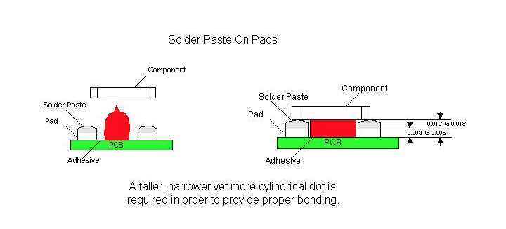
properties. The adhesive selected should be formulated to allow for a
higher profile dot that exhibits very little slump. This will allow the
glue to contact the component, above the height of the solder paste
deposition, when the component is placed. Dots dispensed for this type
of application should have a tall, cylindrical shape as opposed to the
typical triangular Hershey kiss dot profile. The typical profile may
not allow the glue to properly adhere to the component prior to curing
and then hold the component through wave soldering. This will cause a
large number of missing component errors to be seen following the wave
soldering operation. Excessive missing components following manual
assembly may also be seen because the glue joint is not large enough to
provide the strength needed to hold the components in place.

 The surface mount
adhesive chosen for these applications must also have a high green
strength in order to hold the component prior to the curing process. It
is this green strength that also helps the adhesive to maintain the
tall cylindrical dot shape needed when dispensing between solder pasted
pads. Without it the adhesive deposit will slump, losing contact area
with the component, and causing a decrease in the strength of the
adhesive joints.

SMT,THT,PCB,PCBA,AI,wave soldering,reflow oven,nozzle,feeder,wave soldering,PCB Assembly, LED, LED lamp, LED display,


 In adhesive
dispensing processes utilizing heat, it is difficult to achieve the
necessary dot height. By applying heat to the adhesive, the material’s
viscosity is lowered, allowing it to flow more easily. This type of
flow characteristic will cause the adhesive dot to slump after
dispensing. Problems related to the adhesive not contacting the
component (missing components after wave soldering, etc.) will increase
in frequency, as well as the number of opportunities for defects such as
pad contamination to occur.


Board Design

SMT,THT,PCB,PCBA,AI,wave soldering,reflow oven,nozzle,feeder,wave soldering,PCB Assembly, LED, LED lamp, LED display,


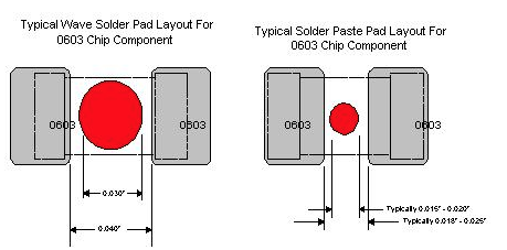
 Typically,
surface mount component pads are designed for either adhesive deposition
or the screening of solderpaste. The pad spacing is generally smaller
for solderpaste application as opposed to that of adhesive deposition.
For example, the component pad spacing between the pads of a 0603 chip
cap/resistor is typically 0.020”, if the board was designed to be screen
printed with solderpaste. The pad spacing for the same board can be
0.040” if adhesive deposition was to be utilized. A 0.030” diameter dot
of adhesive would easily be recommended for use if the component pads
on the board were indeed designed for adhesive deposition. However, if
the pad design for the same board was originally designed for
utilization of solderpaste, as a method of adhering the component to the
board, obviously, an 0.030” diameter dot of adhesive would be too
large, as the spacing between the pads is now 0.020”. A 0.015” to 0.018”
diameter dot is required for this particular application.

 In designing pad
spacing and component spacing, the height of the pad and the solder
paste deposition must also be taken into consideration. Typically, the
height of an adhesive dot is one half the diameter of the dot.
Depending upon the material used for the pads, it would be possible
design a board which would be impossible to print and dispense adhesive
on. If the typical dot size for a 0603 component were 0.015” to 0.018”,
the height would be approximately 0.0075” to 0.009”. If the thickness
of the stencil utilized to print the solder paste was 0.006” to 0.007”
this might not allow the glue dot to contact the component body on some
types of board finishes. For example, a typical HASL finish is
approximately 0.003” thick. If the thickness of the stencil utilized
were 0.007”, the adhesive dot would have to be at least 0.011” to 0.012”
tall to properly contact the component. This would require
approximately a 0.022” diameter dot. This is why the rheology of the
adhesive is so important. If the adhesive slumps at all after
dispensing, it may not properly contact the component. The nozzle
design also plays a part in the development of the correct dot for each
application.


Nozzle Design


When selecting a nozzle for use in dispensing adhesives the main characteristics that must be considered are nozzle
design, standoff size and placement, and nozzle ID. A relationship
exists between these characteristics and the adhesive dot diameter.
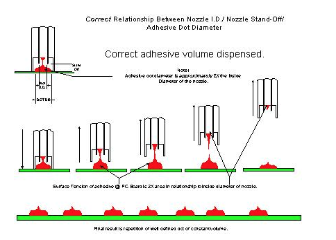
When the adhesive volume is dispensed, the surface tension of the
adhesive on the board, should be twice that of the surface area of the
adhesive at the nozzle tip. If this condition exists, as the nozzle
retracts, the adhesive will snap off clean from the nozzle and leave a
well-defined dot of constant volume on the board. The nozzle must be
chosen based upon the size dot that is required by the application.

SMT,THT,PCB,PCBA,AI,wave soldering,reflow oven,nozzle,feeder,wave soldering,PCB Assembly, LED, LED lamp, LED display,


Nozzle selection
refers in this case to specific nozzle specifications for a known dot
size requirement. The dot size requirements can be derived from the
board design being utilized or specifically the pad spacing of
components. Reference pad spacing previously discussed in this paper. It
is not uncommon for Manufacturing Engineer personnel or Quality
Engineering personnel of a printed circuit board manufacturing facility,
to inquire what a recommended adhesive dot diameter should be for a
particular component type. Much has been written in regards to
recommended surface mount component pad designs and layouts for bottom
side applications. Topside pad designs are also used on bottom side PCB
fabrication. However these guidelines are rarely utilized. The pad
spacing for a particular component for each individual customer product
is unique.

Because the pad
spacing for most typical surface mount components is not standardized
from one customer product to another, it becomes a challenging task when
recommending what tooling should be utilized to satisfy a particular
customers’ adhesive deposition requirement for a particular component.

Note that the
volume of adhesive needed to maintain the component in place during the
high speed placement or wave solder process may be larger than possible
for some specific pad designs.

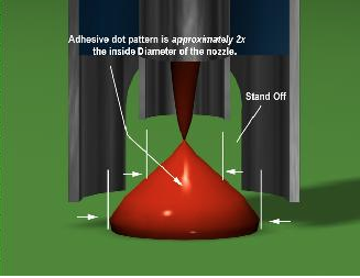
The nozzle standoff
can be defined as the distance from the tip of the dispensing surface
to the end of the mechanical standoff. The nozzle standoff is used to
maintain the distance between the PCB and the dispensing tip. Most
dispensers in use today are designed to utilize some sort of mechanical
standoff with the nozzles. The standoff usually dictates, to some
degree, the height of the dispensed dot

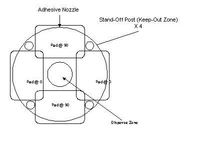
Typical designs for
nozzle standoffs are the castle design, the post design, or a dual post
design. For applications utilizing surface mount adhesive between pads
that have had solder paste applied to them, a single post design nozzle
is the most appropriate. In this type of application the standoff
should be set at 45
° , 135 ° , 215 ° , or 315 ° around the pad circuitry.

SMT,THT,PCB,PCBA,AI,wave soldering,reflow oven,nozzle,feeder,wave soldering,PCB Assembly, LED, LED lamp, LED display, 


When selecting the
correct nozzle ID a rule of thumb is that the nozzle ID should be one
half of the required dot diameter. This will allow for the correct dot
diameter to be dispensed so that the glue snaps away from the nozzle
without contamination. By beginning with this guideline, the
approximate nozzle diameter can be determined, and then adjusted based
upon the material utilized.

SMT,THT,PCB,PCBA,AI,wave soldering,reflow oven,nozzle,feeder,wave soldering,PCB Assembly, LED, LED lamp, LED display,


Stencil Printing Considerations


 When printing
solder paste prior to dispensing surface mount adhesive, there are some
stencil design considerations that must be taken into account. The
thickness of the stencil is important because it will determine the
height of the solder paste depositions. This also determines the
minimum height of the dot that must be dispensed in order to properly
contact and hold the component. In applications where wave soldering
will follow manual assembly, a smaller stencil thickness may be used
because the ultimate solder joint quality will be determined by the wave
soldering operation. It may also be beneficial, on pads with very
tight pads spacing, to undercut the stencil so that as much space as
possible is available for adhesive deposition.


Adhesive Curing


    When printing
solder paste and dispensing epoxy between solder pasted pads a
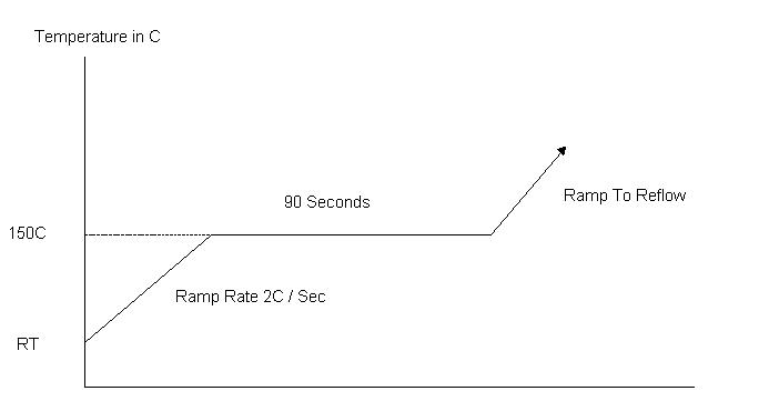
specialized cure cycle is required. Curing epoxy at 150º C is a
bondline temperature that should be verified with thermocouples at
various locations. Curing epoxy at temperatures above 160º C can cause
the adhesive to become brittle, leading to possible component loss
during the solder wave process. The solution for this is that the epoxy
must be cured at 150º C for about 90 seconds prior to ramping to the
reflow temp. This type of reflow takes into account the adhesive cure
as well as the solder paste reflow. Care should be taken to check the
quality of the solder joints achieved with this profile. The graph
below is a sample of what the cure cycle should look like. The final
profile should take into account the recommended profiles from both the
adhesive and from the solder paste manufacturers.


SMT,THT,PCB,PCBA,AI,wave soldering,reflow oven,nozzle,feeder,wave soldering,PCB Assembly, LED, LED lamp, LED display,


Placement Machine Considerations


 When selecting a
placement machine for use in a process utilizing the dispensing of
surface mount adhesives between solder pasted pads, it is important to
consider the accuracy and the repeatability of the placement machine
down line. In typical top side applications utilizing solder paste
printing, when the solder paste is reflowed, the forces associated with
the solder, automatically center the component, within reason, on its
pads. When glue is added to the process this does not occur because the
glue resists these forces since it is cured prior to the reflowing of
the solder paste. It is important to consider all of the machines in
the line when developing this type of process.


Typical Manufacturing Line Configurations


Traditional Bottom Side Line

SMT,THT,PCB,PCBA,AI,wave soldering,reflow oven,nozzle,feeder,wave soldering,PCB Assembly, LED, LED lamp, LED display,

  GDM Adhesive Dispenser

  Vitronics Reflow Oven

  HSP Chipshooter


Typically, a
traditional bottom side manufacturing line includes an adhesive
dispenser, a chipshooter to place the bottom side components, and an
oven to cure the adhesive. This line will be followed by a wave solder
machine, which will in turn be followed by an inspection and/or rework
station.
The first thing
that must be considered when setting up any manufacturing line is the
type of components and assemblies that are going to be used or built on
it. A traditional bottom side line can be used simply to apply glue to a
printed circuit board, place components on the board, and then cure the
glue in order to hold the parts onto the board prior and during wave
soldering and manual assembly. In this type of application the green
strength of the material determines whether components stay in place
during placement operation on the chipshooter. The post cure strength
of the adhesive determines whether or not the components will stay on
the board during manual assembly and handling. This makes the choice of
glue very important. After wave solder, using this type of line, parts
may be missing due to missing or unacceptable adhesive dots or some may
have be knocked off the board during manual assembly or handling. Care
should be taken to control the forces that these assemblies are
subjected to. This line is very basic in its functionality but can
reliably build products when implemented correctly.


Bottom Side Line With Solder Paste Application

SMT,THT,PCB,PCBA,AI,wave soldering,reflow oven,nozzle,feeder,wave soldering,PCB Assembly, LED, LED lamp, LED display,


  HSP Chipshooter

  DEK Stencil Printer

  Vitronics Reflow Oven

  GDM Adhesive Dispenser


A bottom side line,
that includes solder paste application, incorporates a system for
applying the solder paste (stencil printer or high speed dispenser), an
adhesive dispenser, a chipshooter for the bottom side components, and an
oven to cure the adhesive and reflow the solder paste. A wave solder
machine and an inspection and/or rework station will then follow this
line.

This type of
manufacturing line is more flexible than the previously discussed line.
For bottom side applications, this configuration provides greater torque
strength due to the adhesive being combined with solder paste. This
will assist in reducing the number of missing part defects present in
the assembly. This type of line also helps to reduce problems related
to the wave soldering operation (insufficient solder). In this type of
application, the dot height is important to consider because the dot
must be tall enough to contact the component even above the solder paste
deposit. Consideration also must be given to the design of the stencil
used to print the solder paste and the design of the nozzle used for
high speed dispensing operations. Both of these points can turn into
problems later if not considered properly.


Mixed Technology Top/Bottom Assembly with Solder Paste Application

 SMT,THT,PCB,PCBA,AI,wave soldering,reflow oven,nozzle,feeder,wave soldering,PCB Assembly, LED, LED lamp, LED display,

      Vitronics Reflow Oven

  HSP Chipshooter

  GDM Adhesive Dispenser

  DEK Stencil Printer

  GSM Flexible Placement


A mixed technology
line for assembling top and bottom side products includes a system for
applying the solder paste (stencil printer or high speed dispenser), an
adhesive dispenser, a chipshooter to place the bottom side components, a
flexible placement machine to place top and bottom side components, and
an oven to cure the adhesive and reflow the solder paste. A wave
solder machine and an inspection station will then follow this line.
The inspection station however, should see limited use because of the
robustness of this process.

This manufacturing
line is more flexible than either of the previously discussed lines.
Like the bottom side manufacturing line with solder paste, on bottom
side applications, this configuration provides greater torque strength
due to the adhesive being combined with solder paste. This assists in
reducing the number of missing parts present in the assembly. This
also helps to reduce problems related to the wave soldering operation
(insufficient solder). In this type of application, the dot height is
important to consider because the dot must be tall enough to contact the
component over and above the solder paste deposit. Consideration also
must be given to the design of the stencil used to print the solder
paste and the design of the nozzle used for high speed dispensing
operations. This line also can be used for topside applications
including the deposition of solder paste, chip placement and flexible
placement (QFPs and BGAs for example). This type of flexible
manufacturing line has become the choice for contract electronics
manufacturers because it offers a simple, total assembly solution.


Conclusion


 The dispensing of
surface mount adhesives has been a part of electronics manufacturing
since the development of surface mount components. In an effort to make
the processes involved more robust, solder paste has been added to many
manufacturing line configurations. This configuration helps to
eliminate defects such as missing components and insufficient solder
joints following wave soldering.

 In order to
implement this process there are a lot of considerations that must be
taken into account. The type of adhesive used must have rheological
properties that allow for a tall, cylindrical dot versus the typical
Hershey kiss shaped dot. This type of dot is required to properly
adhere to the component when it is placed on top of the solder paste
deposits. In order to obtain the correct dot height, the board design
must be considered carefully. By designing in the correct pad spacing,
implementation of this process is much simpler. The volume of solder
paste required must then be determined as well as the design of the
stencil. The required adhesive dot size must be considered when
designing the stencil. After the board is designed and the volume of
solder paste required has been determined, a nozzle must be designed to
provide the correct dot diameter with standoffs that will not become
contaminated with solder paste. After the adhesive is deposited and the
chips have been placed, the glue must be cured and the solder paste
must be reflowed. The profile used for this process must be developed
from the adhesive and the solder paste manufacturers’ recommended
profiles. Finally, the type of assemblies that are going to be built
must be considered when developing a manufacturing line that will meet
your needs now and in the future.

 By carefully
considering all aspects of your manufacturing process, the dispensing of
surface mount adhesives between solder pasted pads can help eliminate
defects associated with typical electronics manufacturing processes.
This process helps to eliminate problems such as insufficient solder
joints. In applications where only glue was previously utilized, this
type of process can help eliminate defects such as missing components,
that can occur as a result of handling and manual assembly. By taking
time to consider the characteristics of your manufacturing process, the
correct line configuration and process parameters can be developed to
build the highest quality assemblies possible.


How to evaluate SMT Auto Insertion machine supplier

Quality System Assessment Summary Report

Supplier:  

Commodity Team:

Primary Audit Contact:

Address:     


Supplier Commodity/Product Specialty:

Audit Team:


Phone: 


Fax: 


Elements


Max.

Audit Date:

Re-audit Date:

/ /

%

Improvement


Physical/ Logistical

Capabilities

(for information only)

Score

(0-3)


Score

Score

Score


A. Geographic location

3

1 Management Responsibility


B. Plant condition / size

3

2 Quality System


C. Employment / labor recruiting

2

3 Contract Review


D. Finance resources

3

4 Design Control


E. Pricing history

2

5 Document and Data Control


F.   Equip. Condition /age / application


2

6      Purchasing and verification


G. Backlog / capacity status

2

7 Customer Supplied Products


Yes/ No for following

8 Product Identification and Traceability

4


H. ISO / QS 9000 certified

Yes

9 Process Control


I. Design Capability

Yes

10 Inspection and Testing


J. Quick turn/prototype capability

Yes

11    Control of Inspection and Test Equip.


12


K. JIT capability / Kanban

Yes

12 Inspection and Test Status

2


13 Control of Nonconforming Product


14 Corrective and Preventive Action

6


Calculations:

15 Handling, Storage, Pack. and Delivery

9


1. Quality System Score (%):

16 Control of Quality Records

5


Total Audit Score x 100

17 Internal Auditing

10


(Total Max. Score – N/A Score)

18 Training

6


2. % Improvement:

19 Servicing

4


(New Score – Previous Score) x 100

20 Statistical Techniques

30


Previous Score

21 Continuous Improvements


Total Score


Auditor’s Signature:   


% Score


Date: