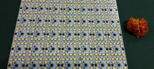
Wave Solder:
Surface wave are covered by a layer of scale, it is in almost all along the length direction of the solder wave, keep the static, in the process of wave soldering, PCB exposure to the forefront of tin wave surface, oxide skin breakdown, in front of the PCB solder wave without being Jun folds forward, indicating that the entire scale and the PCB at the same speed mobile crest welder
Solder joint shape:
When the PCB into the wave front end (A), base plate and pin heated, and before his leave wave surface (B), the whole PCB in the solder, namely by solder bridging, but leave the wave at the moment, A small amount of solder due to the effect of wetting force, adhesion on the bonding pad, and due to the reason of surface tension, there will be A contract for the center with lead to minimum state, at this time between the solder and solder wetting ability than cohesion between two solder in solder. Therefore will form a full, round solder joints, leave the wave at the back of the excess solder, due to the gravity and back
Tin pot.
Prevent bridging:
- Use the solderability good components/PCB
- Improve the activity of welding Ji
- Improve the PCB preheating temperature, increase the solder wetting performance
- Increase the temperature of the solder
- Remove the harmful impurity, reduce the cohesion of solder, to facilitate the solder separated between the two solder joints.
The crest welder common preheating method:
- Air convection heating
- The infrared heater heating
- The method of combining the hot air and radiation heating
Wave soldering process curve resolution:
- The wetting time
Refers to the solder joint and the starting time of the solder wetting after contact
- The residence time
On a PCB solder joints from the wave surface contact to leave wave time below
Stay/welding time calculation is: stay time = wave width/speed/welding
- The preheating temperature
Preheating temperature is refers to the PCB and the temperature reached before the wave surface contact (see right-hand chart)
- Welding temperature
Welding temperature is very important for welding parameters, usually higher than the melting point of solder 50 ~ 60 ° C (183 ° C) ° C for the most part refers to the temperature of the soldering furnace operation, PCB solder joints welded by the temperature is lower than the results of the furnace temperature, this is because the PCB endothermic
SMA type components preheating temperature
Single panel component hole device with conventional 90 ~ 100
Double panel component hole device 100 ~ 110
Double panel component mixed 100 ~ 110
A multilayer through-hole device 115 ~ 125
A multilayer mixed 115 ~ 125
Art and welder peak wave number to adjust:
- The wave peak height
Wave peak height refers to wave soldering PCB solder height. Its numerical control in PCB thickness usually 1/2 ~ 2/3 are exaggerated, solder melt flow will cause, to form a “bridge” on the surface of the PCB
- The transmission Angle
When peak wave welding machine is installed in the device level, should also be necessary to adjust the sexual transmission Angle of dip Angle, by adjusting to the abandoned domestic PCB, but the peak wave Angle of the welding, time, when is suitable for domestic will help more PCB welding fee liquid stripping sex fast, to return to the tin pot
- The cyclone knife
Tens of thousands of boom knife, sma peak wave put down, just left after welding in sma cavity “a long narrow long with open cavity of narrow,” illustrates the blow out hot function form, especially such as knife, therefore calls “sword” boom.
- The influence of solder on the purity
Wave peak during the welding process, welding source solder impurity) Shanghai plate [on PCB, analyse leaching copper will lead excessive copper content in welding defects
- Flux
- The parameters of industrial cooperation > >
Wave peak welding parameter > > industrial tape speed, and time of hot welding the reserved time and mutual cooperation, adjustment Angle of demand.
Wave soldering defect analysis:
- The POOR WETTING POOR WETTING:
This situation is unacceptable defects, only partially wetting on the solder joints. Analyze the reasons and improving ways are as follows:
1-1. External contaminants such as oil, grease, wax, etc., and such pollutants are usually available solvent cleaning, this kind of pollution is sometimes in the printing on the flux.
1-2. SILICON and lubricating OIL are normally used for stripping, usually in the base plate and parts found on his foot, and SILICON OIL is not easy to clean, so use it to be very careful especially when it does antioxidant OIL problems often happen, because it will evaporate to touch on the substrate and cause poor wetting.
Often 1-3.
Storage condition bad or substrate oxidation process on the problem, and the flux can’t remove will cause poor wetting, secondary tin or can solve this problem.
1-4. With flux method is not correct, cause the reason for foaming pressure instability or inadequate, causing unstable foam height or uneven and make the substrate part does not have to touch to the flux.
1-5. Insufficient solder time or tin temperature can lead to poor WETTING, because the temperature of the molten tin need enough time and WETTING, usually soldering temperature should be higher than the melting point temperature 50 ℃ to 80 ℃, WETTING the total time about 3 seconds. Adjust the solder paste viscosity.
- Partial wetting bad:
This situation is similar to poor wetting, different is bad local wetting will show no copper foil surface, only a thin layer of tin can’t form full of solder joints.
- Cold welding or solder joints is not bright,
Solder appears to be broken, uneven, most of the reason is parts solder was cooled in the formation of solder joints caused by vibration, pay attention to the tin stove whether there are abnormal vibration.
- The solder joint failure:
This situation is usually a solder, base plate, guide hole, and the expansion coefficient between parts feet, not cooperate, should be in the base material, improve the parts material and the design.
- Solder tin content is too big:
Usually in the evaluation of a solder joint, the hope can big, round and fat of solder joints, but in fact too much solder joints to electrical conductivity and the tensile strength is not necessarily help.
5 to 1. The tin stove transmission Angle is not correct will cause the solder joint is too big, by the tilt Angle
1 to 7 degrees in accordance with the substrate design approach? # 123; The whole, the general point of about 3.5 degree Angle, Angle, the greater the wetting Angle of the thinner the smaller wetting the more thick.
5 – (2) improve the tin bath temperature, longer soldering time, make the excess tin back into the tin bath again.
5 – (3) improve the preheat temperature, can reduce substrate wetting heat, have added to help welding effect.
5-4. Change the proportion of flux, slightly lower flux density, usually share the higher solder more thick also more easy to short circuit, the lower the proportion of tin solder the thinner but more easily cause bridge, icicles.
- Icicles (icicles) :
This problem usually occurs on the welding process of DIP or WIVE, at the top of the foot parts or had found ice point of tin solder joints.
6-1. The base plate weldability poor, this problem is often accompanied by poor wetting, this problem should explore by substrate weldability, try by flux ratio to improve the ascension.
6-2. Gold on a substrate (PAD) area is too big, can be used
Green (welding) proof paint line dividing gold way to improve that in principle with green (welding) proof paint line in daikin pavement separated into 5 mm by 10 mm block.
6 – (3) lack of tin bath temperature wetting time is too short, can be used to improve extension soldering tin bath temperature time, make the excess tin back into the tin bath to improve again.
6-4. After a wave of cool wind flow Angle is wrong, is blowing in the direction of the tin bath, will cause the solder point rapidly, excess solder cannot be affected by gravity and cohesion back to the tin bath.
6-5. Generated when the hand soldering tin peak, usually for the solder iron temperature is too low, inadequate to soldering temperature to solder joint formed by the cohesion bounce back immediately, switch to a larger wattage soldering iron, lengthen the iron in the preheating of the object being welded.
- The welding on the green paint with remnants of tin:
7-1. The base plate production residues have some with flux can’t compatible materials, overheating in the 餪 turn produce sticky stick after soldering tin wire, usable acetone (* chemical solvent has been disable the Montreal convention), and chlorinated solvents such as alkene to clean, if still can’t improve after cleaning, has the possibility of CURING substrate layer material is not correct, this accident should be timely feedback substrate suppliers.
7-2. Incorrect substrate CURING can cause this phenomenon, two hours before plug-in first bake 120 ℃, the project accident should be timely feedback substrate suppliers.
7-3. Tin tin slag is PUMP into the slot and then spray out the base plate surface with tin slag, caused this problem is relatively simple maintenance good tin furnace, tin tin bath right level (normal conditions when tin tin slot jet still not face away from the edge of tin bath 10 mm height)
- White residue:
After welding or solvent cleaning found a white residue on the base board, usually the remains of the rosin, this kind of matter will not affect the surface resistance is qualitative, but customers don’t accept it.
8-1. The problem of flux is usually the main reason, sometimes to switch to another flux can be improved, rosin type flux often produce work days, when the cleaning at this time the best way is to seek the assistance of flux suppliers, products is that they supply them more professional.
8 – (2) substrate residual impurities in the process of production, also can produce white spot under long-term storage, available flux or solvent wash.
8-3. Incorrect CURING also can cause the day, is usually a batch separately, should be timely feedback base board and the supplier use flux or solvent wash.
8-4. The factory using the flux and the base board of oxidation layer is not compatible, had occurred in the new substrate suppliers, or change the flux label, should ask the supplier to assist.
8-5. In case of substrate process used in the solvent to change the base material, especially in the process of nickel plating solution often cause this problem, suggestion storage time as short as possible.
8-6. Flux used for aging, exposed to the air absorbs moisture degradation, suggest update flux (usually foam type flux should be updated every week, immersion flux is updated every two weeks, spray monthly update).
8 to 7. The use of rosin flux, after soldering furnace hou parking time is nine to cleaning, cause the day shift, as far as possible to shorten the time of soldering and cleaning can be improved.
8 and 8. Solvent cleaning the substrate moisture content is too high, reduces the cleaning ability and produce day. Should update the solvent.
- Dark residue and etching trace:
Usually black residue had occurred in the bottom of the solder joint or at the top, this problem is usually incorrect use of flux or cleaning.
9-1. Rosin flux welding did not immediately after cleaning, dark brown left, to wash in advance as much as possible.
9-2. Acid flux on the solder joints caused by black color, corrosion and not cleaning, this phenomenon in the welding often found that switching to the flux of the weaker and cleaning as soon as possible.
9-3. Organic flux at high temperature burning, resulting in the class, to confirm the tin bath temperature, switch to more resistant to high temperature flux.
- Green residues:
Green usually is caused by corrosion, especially the electronic products but is not entirely true, because it is difficult to distinguish what is green rust or other chemical products, but generally found that green stuff should be warning, must immediately find out the reason, especially the green material will be more and more big, should pay attention to very much, usually available to improve the cleaning.
10 to 1. The corrosion problem
Usually occurs on the bare copper or copper alloys, the use of rosin flux, the corrosion substance containing copper ions so green, when found the green corrosion and can be proved after the use of rosin flux is not properly cleaned.
10-2. COPPER ABIETATES is COPPER oxide and ABIETIC ACID compounds (rosin main component), the material is green, but never is corrosive and high insulation, do not affect quality but the customer will not agree to clean.
10-3. PRESULFATE residue or similar residue substrate production, produce green residue after soldering, the base board manufactory should be asked substrate cleaning degree and then do test, to ensure the quality of the base board cleanliness.
- White corrosion:
8 talking about white residue is refers to the substrate white residue, and the project talking parts foot and white on metal corrosion, especially lead composition more easily into such residues on the metal, mainly because of chloride ion is easy to form lead chloride with lead, lead again with carbon dioxide to form carbonic acid corrosion (white). When the use of rosin flux, for rosin will does not dissolve in water containing chlorine surfactant wrapped from corrosion, but if use undeserved solvent, clean rosin can not only remove chlorine ion, thus has accelerated corrosion.
- The pinhole and the porosity:
Pinhole and the porosity of the difference, pinhole is to find a small hole in the solder joints, porosity is larger hole on solder joint can be seen inside, it is empty normally in the pinhole internal, internal air porosity is completely out and cause the size of the hole, the forming reason is solder in the gas has not been completely ruled out that has solidified, and form the problem.
12-1. Organic pollutants: base board and parts
Foot caused pinhole or porosity, gas may be produced its pollution source may come from planting a machine or storage condition, the problem is simple as long as the solvent wash, but such as contaminant SILICONOIL because its not easy to be solvent cleaning, therefore, should be considered in the process of other substitutes.
12-2. Substrate moisture: such as using the base material of cheaper, or use a rough way of drilling, the penetration hole easy absorption of moisture, soldering process caused by high heat evaporates, the solution is two hours at 120 ℃ baking in the oven.
12-3. The plating brightener in the solution: use a large amount of brightener, electroplating brightener with gold deposit at the same time, the high temperature caused by the volatile, especially when the gilded, switch to plating solution containing less brightener, of course it will feedback to suppliers.
- TRAPPED OIL:
Oxidation prevent oil Wells into Canon of tin bath flow and pollution substrate, this problem should be tin bath soldering fluid level is too low, additional soldering tin groove can be improved.
- Solder gloomy:
This phenomenon can be divided into two (1) for a period of time after soldering, solder joints (about half cargo to one year) turn dark color. (2) the manufactured product solder joints is grey.
14-1. The soldering the impurity: every three months must regularly test the metal ingredients inside the solder.
14-2. Flux on the surface of the heat will also have some degree of grey color, such as RA and the flux of organic acids on the spot for too long can cause slight corrosion and a grey colour, immediately after welding cleaning can be improved. Some inorganic acids can cause any ZINC flux OXYCHLORIDE available 1% hydrochloric acid cleaning and washing.
14-3. In solder alloy, tin residency content (such as 40/60 solder) solder joints in gray.
- Solder surface roughness:
Solder surface sand with prominent surface and the solder joint shape does not change as a whole.
15 to 1. The crystallization of metal impurity: every three months must regularly test the metal ingredients inside the solder.
Was 15-2. Tin slag, tin slag PUMP Wells into the Canon of tin bath jets for tin contains tin slag and make the solder surface of sand form, shall be the tin bath soldering fluid level is too low, tin groove add solder and should clean up the tin bath and the PUMP can be improved.
15-3. The foreign substances, such as flash, insulation materials, such as hidden in parts, also can produce a rough surface.
- Yellow spot:
Due to soldering temperature is too high, see if tin and temperature thermostat failure immediately.
- A short circuit:
Too much solder joints caused by two solder joints.
17-1. The solder didn’t have enough time, substrate preheating insufficient adjustment tin stove.
17-2. Flux bad: improper flux density, degradation, etc.
17-3. The substrate with tin wave direction and harmful, solder direction changes.
17-4. Bad circuit design: lines or contact between too close () should be more than 0.6 mm spacing; Such as array type solder joints or IC, should consider to steal soldering pad, or use white paint to separate words, at this time of white paint thickness for more than 2 times the thickness of welding pad (gold).
17-5. The contaminated tin or excessive accumulation of oxide by PUMP wear caused by short circuit should clean up the tin stove or further update all soldering tin groove.