Why It Is Good to Invest In Machines?

Most of our customers use financing rather than capital outlays to grow their manufacturing business, and they have a number of smart reasons for doing so:

1. CHEAPER THAN CONTRACTING YOUR ASSEMBLY OUT

Companies can spend $10k and more a month contracting out their manufacturing, but you can typically bring an SMT assembly line in-house for a third of that when you lease or finance your line, and many companies already have a person on payroll who can operate the equipment.

2. EASIER TO GET THE GO-AHEAD

Financing typically requires fewer internal approvals than a capital purchase, making it the faster and easier route to an assembly line install or upgrade.

3. INCREASE YOUR PRODUCTION CAPABILITY SOONER THAN LATER

Rather than waiting until the money is there for a major capital outlay, with financing you can start the ball rolling on ordering, receiving, and installing your new equipment right away, allowing your company to benefit from increased capacity and capability much sooner than you might have otherwise.

4. GET BETTER EQUIPMENT

Financing gives you more purchasing power than a cash purchase. This means you can focus more on your goals than your budget.

5. ROLL IN INSTALLATION AND TRAINING

With a cash purchase comes the temptation to reduce costs, sometimes causing essential aspects like installation and training to be cut, but installation and training can have a big impact on how quickly your new equipment or production line gets up and running. Financing allows you to roll this cost into your payments.

6. PRESERVE YOUR WORKING CAPITAL

Making a large cash investment in your production line leaves you with less ability to put that money to other strategic uses, such as growing sales and increasing inventory.

7. IMPROVE CASH FLOW AND EXPENSE PLANNING

With financing, your new equipment becomes a regular monthly expense item in the budget.

8. OBSOLESCENCE PROTECTION

At the end of your lease term, equipment can be purchased at fair market value, upgraded, or swapped.

Common Failures and Maintenance of Reflow Oven

Introduction

  • The industrial ovens used to reflow solder on a printed circuit board are intricate tools. Using a combination of radiated heat and heat convection, the solder reflow oven delivers a carefully regulated flow of consistent heat to the PCB. This process completes the assembly of the board by melting the solder to form good solid solder joints between the components and the board.

Failures and Maintenance

  • When the red light is on, the buzzer long beeping non-stoppably
    Cause: Control buzzer time relay does not work; control thermocouple opens circuit; control section of the main circuit SSR is damaged.
    Solution: Check the control buzzer time relay; check the control thermocouple; check the control section of the main circuit SSR.
    2. The system automatically enters the cooling state
    Cause: PCB dropped or jammed; transport inlet and outlet electric eye damaged.
    Solution: Take out the dropped board; replace the electric eye.
    3. The start-up process heating area temperature does not rise to the set temperature
    Reason: Damaged heater; Heating point pair faulty; Solid state relay output disconnection; Exhaust too large or unbalanced left and right exhaust; Damaged photoelectric isolation device on the control board.
    Solution: replace the heater; check or replace the electric thermocouple; replace the solid-state relay; adjust the exhaust valve air plate; replace the opto-isolator.
  • Emergency switch pressed, the system is in the waiting state
    Cause: Emergency switch is pressed; line is damaged.
    Solution: Reset the emergency switch and press the start button; repair the circuit.
  • Inaccurate counting
    Cause: The sensing distance of the counting sensor is changed; the counting sensor is damaged.
    Solution: Adjust the sensing distance of the counting sensor; replace the counting sensor.

Cautions

  • Reflow oven must completely reach the set temperature (green light on) before starting to solder.
  • In the reflow soldering process, observe the temperature change in each temperature zone often, the change range is 1 ℃ (according to the reflow oven).
  • When abnormalities occur in smt reflow production, stop it immediately.
  • The size of the substrate should not be larger than the width of the conveyor belt, otherwise cardboard accidents are likely to occur.
  • Before reflow soldering, based on documents or component packaging instructions, the components can not withstand the normal welding temperature must be taken protective measures (shielding) or not be processed by reflow soldering, instead by post-welding with manual welding, or welding robot.
  • In the reflow soldering process, prevent vibration of the conveyor belt, otherwise it will cause displacement of components and disturbance of the solder joint.
  • Regularly measure the amount of air exhausted at the reflow oven vent, the amount of air exhausted directly affects the soldering temperature.

Analysis of AVG market in PCB industry

At present, the automation level of the overall industry processing technology is average, mainly because the special equipment is relatively mature. First of all, small and medium-sized enterprises (small batches of products, many types, too large size range, etc.) have a low level of automation, mainly focusing on special process equipment + retractable board + labor. The medium and large enterprises (large batches, relatively uniform types and specifications) have a higher level of automation, mainly focusing on special process equipment + retractable boards + industrial robots, with manual assistance (inspection, maintenance).

On the whole, the demand for automation transformation of small and medium-sized enterprises is still relatively weak, while medium and large enterprises are on the contrary. Whether it is a newly planned workshop or an upgrade of an old production line, they are actively planning the participation of robots (industrial + AGV), aiming at PCB upstream. Raw materials need to build smarter warehousing; for the PCB factory, a more complete automatic warehousing system is needed, and it is best to integrate ERP, MES, etc.

Although the reality varies widely, automation and intelligence are still the general direction of development. As the basis for the development of the electronics industry, the scale and market of PCB materials and PCB boards will continue to grow with the development of 5G, smart cars, etc. Therefore, the requirements for product quality and process accuracy are higher, and automation and intelligent production scheduling will continue to grow. Demand will continue to rise.

Secondly, there are various types of products in the PCB industry, and the raw materials of the board are large and heavy. The effective transportation and management of semi-finished products or finished products during processing can improve production efficiency, so the level of automation should also be improved.

Whether it is from the perspective of product iteration or technological innovation, the automation transformation of the PCB industry is inevitable, and the efficiency and precision of industrial robots make it an important step in the transformation and upgrading of the industry.

(1) Demand characteristics:
①Industry production characteristics:
A. complex process
B. Work across floors and areas
C. Cancellation in the middle, expedited order
②Environmental requirements:
A. Workshop dust-free level requirements
B. Hydraulic structure (oil leakage)
③Line-side warehouse planning: line-side warehouse design, zoning management, and balanced production of upstream and downstream processes
④Transition period of production and commissioning:
A. There is no MES docking in the early stage;
B. Post-demand docking with MES/ERP/elevator control system
(2) The PCB industry is dedicated to the product form of intelligent AGV
Set up different vehicles for different scenarios to meet the loading requirements (the vehicle is determined according to the customer’s site, and the chassis structure of the vehicle is as consistent as possible). The application model can be selected according to the actual scene needs.

(3) Key technical difficulties related to product selection related benefits:
① The AGV needs to realize cross-regional transfer
● The AGV realizes automatic loading and unloading of production materials through automatic connection with Loader & Unloader;

● The AGV scheduling system is connected with the automatic door controller to realize cross-regional transfer of materials;
● Manage WIP line side warehouse material information to achieve accurate material supply.
② The AGV needs to realize cross-floor transfer;

● The AGV realizes automatic loading and unloading of production materials through automatic connection with the retractable trigger;
● The AGV scheduling system is connected with the hoist controller to realize cross-regional transfer of materials.

(4) Project benefit assessment
Five evaluation dimensions of project benefits: the proportion of production efficiency improvement, the proportion of operating cost control, the degree of shortening the product development cycle, the proportion of product defective product rate reduction, and energy utilization efficiency.

The future development direction of the four PCB markets

Because PCBs (printed circuit boards) are so versatile, even small changes in consumer trends and emerging technologies can have an impact on the PCB market, including how it is used and manufactured.

Although there may be more time, the following four major technology trends are expected to maintain the leadership of the PCB market for a long time and lead the entire PCB industry in different directions.

1- High Density Interconnection and Miniaturization

When computers were first invented, some people probably spent their entire lives getting work done on computers that took up entire walls. And today, even calculator watches have orders of magnitude more computing power than those behemoths, let alone smartphones.

The entire manufacturing industry is currently in the sight of a whirlwind of innovation, much of which is in the service of miniaturization. Our computers are getting smaller and everything else is getting smaller.

Across the consumer base, there seems to be a gradual shift towards smaller electronics. Miniaturization means we can build smaller, more efficient homes and control them. And cheaper, more efficient cars and more.

Since PCBs are vital basic components in electronic products, PCBs must also relentlessly pursue miniaturization.

Especially in the PCB market, this means using high-density interconnect technology. Further improvements in HDI technology will further reduce the size of PCBs and touch more and more industries and commodities in the process.

2- Advanced Materials and Green Manufacturing

Nowadays, the PCB industry is being affected by some very real impacts such as climate and social pressure. The PCB manufacturing process needs to keep up with the trend of the times and evolve towards sustainable development.

In fact, PCB manufacturers have always been a hot topic when it comes to the crossroads of development and environmental protection. The introduction of lead-free solder, for example, required more energy-intensive manufacturing processes. Since then, the industry has been forced to find a new balance.

In other respects, PCB has been leading the way. Polychlorinated biphenyls have traditionally been made using fiberglass as a substrate, which is considered by most to be a relatively environmentally friendly material. Further advancements could see fiberglass replaced by materials better suited for high data transfer rates, such as resin-coated copper and liquid crystal polymers.

As manufacturing efforts of all types continue to adjust their footprints to a changing planet, the link between societal needs and the convenience of production and business will become a new norm.

3- Wearables and Pervasive Computing

We’ve briefly covered the fundamentals of PCB technologies and how they enable greater complexity on thinner boards. Now we put this concept into practice. PCBs are decreasing in thickness and increasing in functionality every year, and now we have a lot of practical applications for small circuit boards.

Consumer electronics as a whole has been a significant driver of PCB manufacturing and usage over the past few decades. Now that wearables have entered this space and are starting to become a reliable consumer product type, related PCBs will follow.

Like smartphones, wearable tech requires printed circuit boards, but they go a step further. They place an emphasis on design efficiency far beyond what past technologies have been able to achieve.

4- Health Medical Technology and Public Oversight

The introduction of modern digital technologies into medicine has been one of the greatest developments in recent human history. Technology now means we can store patient records securely in the cloud and manage them through apps and smartphones.

However, the rapid development of medical technology has also affected PCBs and vice versa in some very interesting ways. The onboard camera is a new development, and it is even possible to fasten an ultra-high fidelity camera to the PCB itself. The medical implications are huge: When a camera needs to be inserted into the body, swallowed by the body, or otherwise introduced into the body, the smaller the better. Some onboard cameras are now small enough to be swallowed.

As for public surveillance, onboard cameras and smaller PCBs can also assist. For example, dash cams and vest cameras have shown useful roles in mitigating offenses, and a number of consumer technologies have emerged to meet this need. Many popular mobile accessory companies are exploring ways to offer drivers increasingly smaller, less obtrusive in-dash cameras that include and include connected hubs to interact with your phone while you’re driving.

New consumer technologies, advances in medicine, breakthroughs in manufacturing, and strong contemporary trends are fascinating. Incredibly, the PCB has the opportunity to be at the heart of it all.

That means entering the field is an exciting time.

In the future, what other technologies will bring new development to the PCB market? Let’s keep looking for answers.

3D SMT machine drawing supporting Smart EMS factory

The unit loads your production line automatically by pushing PCB’s out of a magazine onto the conveyor of the down-stream machine


[embeddoc url=”https://www.smthelp.net/wp-content/uploads/2020/07/SMThelp-PCB-Conveyor-3D.pptx” download=”all” viewer=”microsoft”]

3D RS-1 Vibration Feeder

3D SMT PCB conveyor

3D SMT PCB Magazine

3D Southern Machinery logo

3D UIC Radial taped feeder housing

3D JUKI Gripper nozzle

How to make SMT stencil by Laser cutting machine for EMS factory

[embeddoc url=”https://www.smthelp.net/wp-content/uploads/2020/05/SMT-stencil-laser-making-machine.pdf” download=”all”]SMT stencil production process (reference)

General technical requirements:
1. Screen frame: The frame size is determined according to the requirements of the printing machine. Taking DEK265 and MPM UP 3000 as an example, the frame size is 29ˊ
29ˊ, using aluminum alloy, frame profile specification is 1.5ˊ 1.5ˊ.

  1. Stretching the net: Adopt the red glue + aluminum tape method, at the junction of the aluminum frame and the glue, a layer of protective paint must be evenly scraped. At the same time, in order to ensure that the screen has sufficient tension and good flatness, it is recommended that the stainless steel plate be kept 25mm-50mm away from the inside of the screen frame.
  2. Reference point: According to the size and shape provided by the PCB information, the opening is 1: 1, and the translucent is engraved on the reverse side of the printing. At the corresponding coordinates, the entire PCB opens at least two reference points.

  3. Opening requirements: 1.41. The position and size ensure a high opening accuracy, and the opening is strictly in accordance with the prescribed opening method. 1.42. The size of the independent opening cannot be too large, the width cannot be greater than 2mm, and a 0.4mm bridge is required in the middle of the pad size greater than 2mm, so as not to affect the strength of the stencil.
    1.43. The opening area must be centered.

  4. Characters: In order to facilitate production, it is recommended to engrave the following characters in the lower left or lower right corner of the screen: Model; T; Date; the name of the company that made the screen.

  5. Stencil thickness: In order to ensure the amount of solder paste printing and welding quality, the surface of the stencil is smooth and even, and the thickness is uniform. The stencil thickness refers to the above table. The stencil thickness should meet the premise of the finest pitch QFP BGA. If there are 0.5mmQFP and CHIP 0402 components on the PCB, the stencil thickness is 0.12mm; if there are 0.5mmQFP and CHIP 0603 or more components on the PCB, the stencil thickness is 0.15mm;

The opening shape and size requirements of printed tin screen:

  1. General principle: According to the requirements of the IPC-7525 steel mesh design guide, in order to ensure that the solder paste can be smoothly released from the opening of the stencil to the PCB pad, in the opening of the stencil  to view polyester 1. The area ratio / width-to-thickness ratio area ratio is greater than 0.66 2. The mesh hole wall is smooth. Especially for QFP and CSP with a pitch of less than 0.5mm, suppliers are required to perform electro-polishing during the manufacturing process. 3.) With the printing surface as the upper side, the lower opening of the mesh opening should be 0.01mm or 0.02mm wider than the upper opening, that is, the opening is inverted tapered, which facilitates the ineffective release of solder paste and reduces the number of times of cleaning the stencil. Normally, the size and shape of the opening of the SMT element is the same as the pad, and the opening is 1: 1. Under special circumstances, for some special SMT components, the size and shape of the screen openings are specified.
    No. 2 Special SMT component screen opening:

2.1CHIP components: CHIP components above 0603, in order to effectively prevent the generation of tin beads.

2.2SOT89 components: Due to the large pad and small pad spacing between components, soldering quality problems such as tin beads are prone to occur.

2.3 SOT252 component: Because SOT252 has a large pad, it is easy to produce tin beads, and the reflow soldering tension causes displacement.
Look 2.4IC: A. For the standard pad design, PITCH》 = 0.65mm IC, the opening width is 90% of the pad width, and the length is unchanged.
B. For the standard pad design, IC with PITCH <= 005mm, because of its small PITCH, it is easy to produce bridging, the length direction of the steel mesh opening is unchanged, the opening width is 0.5PITCH, and the opening width is 0.25mm.
2.5 Other situations: One pad is too large, usually one side is greater than 4mm, and the other side is not less than 2.5mm, in order to prevent the generation of tin beads and displacement caused by the effect of tension, the mesh opening is recommended to be divided by grid lines In this way, the grid line width is 0.5mm and the grid size is 2mm, which can be evenly divided according to the pad size.

The shape and size requirements of the opening of the printed rubber screen: glue is used for simple PCB assembly. Dispensing is preferred. CHIP, MELF, SOT components are printed through the screen, and IC is used to avoid glue scraping. Here, only the recommended opening size and opening shape of CHIP, MELF and SOT offset printing plates are given.
1. Two diagonal positioning holes must be opened at the diagonal of the stencil. Select FIDUCIAL MARK to open the hole.

  1. The openings are all elongated. Inspection method 1) Visually check that the opening is centered and the net is flat. 2) Check the correctness of the stencil opening through the PCB entity. 3) Examine the length and width of the screen opening and the smoothness of the hole wall and the surface of the steel sheet with a scaled high power microscope. 4) The thickness of the steel sheet is verified by detecting the thickness of the solder paste after printing tin, that is, the result verification. Conclusion The technical requirements for screen design have been tested for a period of time, and the print quality has been well controlled. The PPM of SMT welding quality has dropped from about 1300ppm to about 130ppm. Due to the development of the packaging direction of modern electronic components, higher requirements have also been placed on the design of steel mesh. Is a subject that we need to focus on in the future


SMT Defects Analysis and Solutions (2020 Essentials)

There are many types of defects in SMT solder joints, and their shapes are also various. Common SMT solder joint defects are:
1. (cold soldering) 2. (lcicle)
3. (pseudo soldering) 4. (void)
5. (soldering balls) 6. (open soldering)
7, (excursion) 8, (solder-off)
9, (Set component) 10, (turn)
11, (solder wrong) 12, (flux residue)
13, (solder skips) 14, (solder crazeing)
15, (reverse) 16, solder bridge)
17. (excess solder connection)
18. (insufficient solder connection)

Cold soldering: The solder at the soldering point does not reach its melting point temperature or the soldering heat is not enough, so that it is solidified before wetting or flowing, and no metal alloy layer is formed at all, so that the solder is completely or partially in the amorphous strong state. It is simply deposited on the surface of the welded metal.

Reasons: 1. The heating temperature is not suitable;
2. Deterioration of solder paste;
3. Excessive preheating, long time or high temperature;
4. Due to the surface pollution, the flux capacity is controlled;
5. Insufficient flux capacity.
solution:
1. Adjust the temperature curve of reflow soldering;
2. Replace with new solder paste;
3. Improve preheating conditions;
4. Surface contamination on and around the pads or pins will depend on the ability to control the flux and lead to incomplete reflow, which should be solved by an appropriate post-plating cleaning process;
5. Insufficient flux capacity will result in incomplete removal of metal oxides, and then incomplete coalescence, similar to surface contamination.

Virtual soldering (non-wetting or semi-wetting): Partial or all of the solder and the surface of the metal being welded do not form an alloy layer, or the metal plating of the lead / solder electrode electrode is peeled off, which causes the lead / solder end and the pad The phenomenon of unstable electrical line isolation occurs between the two, causing the electrical connection to be either on or off.

the reason:
1. Poor solderability of components and pads;
2. Poor quality of solder alloy or solder powder;
3. Poor flux activity;
4. Improper reflow temperature and heating rate;
5. The printing parameters are incorrect.
solution:
1. Strengthen the selection of PCB and components, temperature and humidity control;
2. Impurities such as aluminum, cadmium, or arsenic in the solder can cause poor wetting. The irregular shape of the solder powder also reflects a large oxide content, which consumes more flux and causes poor wetting. Obviously, poor wetting is caused by poor flux activity;
3. Adjust the temperature curve of reflow soldering (reflow time, temperature and reflow gas have a great influence on the wetting performance, or the heat is insufficient due to too short time or too low temperature, resulting in inadequate flux reaction Complete and incomplete metallurgical wetting reactions produce undesirable wetting. On the other hand, the excessive heat before the solder melts not only excessively oxidizes the pad and lead metals, but also consumes more flux;)
4. Reduce the viscosity of the solder paste, and change to increase the pressure of the scraper and slow down the speed.

Tin Bead: Excess bead solder that adheres to the substrate or components and other parts of uneven size solder joints.

the reason:
1. Generally, the poorly printed board or solder paste is mixed with moisture, which will form when the welding is heated;
2. Environmental impact, temperature (the optimal temperature for solder paste printing time is 25 ℃ ± 3 ℃, and the relative humidity should be 60%. The temperature is too high, the solder paste easily absorbs water vapor, and solder balls are generated during reflow soldering. 😉
3. Temperature curve;
4. The problem of the steel mesh template is too thick and the opening is too large.
solution:
Technology:
1. Reduce the thickness of the steel mesh template;
2. Reduce the size of the hole;
3. Use a hole design that can print less solder paste under the components;
4. Increase the interval between printed solder pastes;
5. Reduce the width of the pad so that it is narrower than the width of the component;
6. Reduce the preheating heating rate (temperature rise should not be too fast, generally should be less than 1.5 ℃ / S, too fast will easily cause splashing and form tin beads);
7. Reduce the preheating temperature;
8. Reduce the pressure of placing components;
9. Pre-bake components or PCB before use.
Materials:
1. Use flux with lower activation temperature;
2. Use a higher amount of solder paste;
3. Use coarse powder solder paste;
4. Solder paste using low oxide solder powder;
5. Use less collapsed solder paste;
6. Use solvents with appropriate vapor pressure.

Offset: It is also considered to be a drift, which is the movement of components on the horizontal plane, resulting in misalignment of components during reflow.

the reason:
1. Machine coordinate offset;
2. The components are lifted by high-density thermal fluid during reflow soldering;
3. The pad design at both ends of the chip component is unbalanced;
4. The width and area of ​​the metal layer of the components are too small;
5. Poor solderability of the metal plating of the component pins;
6. The pad is too narrow.
solution:
Process or design:
1. Correct the program coordinates;
2. Reduce the heating rate during reflow soldering;
3. The pad design at both ends of the balanced chip component, including pad size, heat distribution, heat sink connection, and shadow effect;
4. Increase the width of the pad;
5. Reduce the pollution level of components and metal layers of printed boards, and improve storage conditions;
6. Reduce the thickness of solder paste printing;
7. Pre-dry the solder paste before reflow to reduce the flux outflow rate.
Materials:
1. Use flux with lower outgassing rate;
2. Use flux with lower wetting rate;
3. Use solder paste with delayed melting characteristics, such as a solder alloy composed of tin powder and lead powder.

Vertical piece (tombstone): also known as Manhattan effect, suspension bridge effect or Stonehenge (stone suspension) effect, which is caused by unbalanced wetting of both ends of the component during reflow. (The gravity F1 of the chip component, the vertical vector F2 generated by the surface tension of the molten solder below the chip component, and the vertical vector F3 generated by the surface tension of the surface of the molten solder on the right side of the chip component; both the F1 and F2 forces are pulled down The force is used to keep the components in the proper position, but F3 presses on the corner of the chip component, it will tilt the component to a vertical position. When the force F3 exceeds the sum of F1 and F2, a tombstone occurs .)

the reason:
1. The placement position is shifted;
2. The flux in the solder paste floats the component;
3. The thickness of the printed solder paste is not enough;
4. The heating speed is too fast and uneven;
5. The pad design is unreasonable;
6. Poor solderability of components.
solution:
Process or design:
1. Adjust printing parameters and placement position;
2. Use solder paste with a small amount of solder;
3. The metal terminals under the chip components use a larger width and area;
4. Reduce the width of solder pads;
5. Minimize the uneven distribution of heat, including the connection between the pad and the heat dissipation layer;
6. Through the appropriate PCB design and reflow method selection, the shadow effect is reduced to a minimum;
7. Use organic solderability protector (OSP) or nickel / gold (Ni / Au) coating or tin SN coating on the copper pad instead of Sn-Pb coating;
8. Reduce the pollution and oxidation level of the metal layer of the component terminal or the metal layer of the PCB pad;
9. Use thinner solder paste printing thickness;
10. Improve the accuracy of component placement;
11. Use a gentle heating rate during reflow;
12. Pre-dry before reflow or use a curve with a long-term soaking zone to reduce the outgassing rate of flux;
13. Use a very slow heating curve when crossing the solder melting temperature.
material:
1. Use flux with a slower wetting rate;
2. Use flux with slower outgassing rate;
3. Use delayed-melting solder paste, such as a mixture of tin powder and lead powder or a wide paste alloy.

Misweld: It means that the components or wires welded at the welding place do not meet the design requirements (one or more of them). For example, the variety, specifications, parameters and phase of the components (referring to the reverse or misalignment of electrodes).
Cause: The cause is often the error of the mounting process, which is not detected before welding. Such as wrong materials, wrong coordinates in the program, etc.
solution:
1. Strictly follow the requirements of the program documents;
2. Hand repair parts strictly follow the hand repair program control program operation;
3. The patch coordinates of Teaching machine must be accurate, corresponding to the corresponding position of BOM.

Leak welding: where welding is required without welding (small parts)
the reason:
1. The cause is generally that the solder is not fully reached or not applied, the solder is insufficient and the equipment is the cause;
2. The steel mesh is blocked;
3. The production process is wiped out by man;
4. Mounting problems of machinery and equipment;
5. The problem of Feida’s absorption.
solution:
1. The 2D setting of the tin printing machine needs to be opened;
2. The soldering machine opens the solder paste to add an alarm setting. During the alarm, the operator needs to observe whether the amount of solder paste is enough, and shovel the solder paste on both sides of the scraper into the printing range of the scraper. (The amount of solder paste rolling is a one-dollar coin Diameter is better;)
3. The less the plate is moved by man-made during the production process, the better. If you really want to touch the plate, you should pay attention to the tightness of the sleeve to avoid wiping the sleeve with solder paste
4. The placement height of the nozzle of the placement machine is set. If the component is too high, if it is not covered by the solder paste, it will be easily vibrated or thrown away when moving; at the same time, it is necessary to pay attention to the setting of vacuum suction, (component placement After the alarm is relied on vacuum recognition and camera recognition, the vacuum setting is improper, and the lens is misrecognized because of the long-term use of the nozzle. The device will not alarm after the component is pasted, and will continue to operate, resulting in missing parts;
5. The feeder center of Feida is wrong. When the equipment is sucking materials, the suction is biased, and the components are thrown away during high-speed operation.

Reverse: Polarized components do not correspond to the polar position on the PCB
the reason:
1. The material is reversed;
2. Hand-fixed components are reversed or reversed;
3. The mounting angle or recognition angle of the machine component is set incorrectly.
solution:
1. Strictly follow the requirements of the program documents;
2. Hand repair parts strictly follow the hand repair program control program operation;
3. Normally, the identification angle of the component is set to 0. The mounting angles of the component are Panasonic and YAMAHA, which are set counterclockwise, and Kyushu Panasonic is set clockwise. Set the polarity of the component to the PCB. In the same position.

Bridging (connecting to tin or short circuit): There is solder adhesion between two or more solder joints that should not be connected, resulting in undesirable electrical connection or short circuit.

the reason:
1. The solder paste collapses;
2. Too much solder paste is too thick;
3. The heating speed is too fast;
4. Excessive component placement pressure;
5. Stains of solder paste.
solution :
1. Increase the solder paste metal content or viscosity, and replace the solder paste;
2. Use thinner steel mesh template (generally 5-6Mil) staggered hole pattern, or reduce the size of the window hole to reduce the amount of solder paste or reduce the pressure of the scraper;
3. Adjust the reflow soldering temperature curve, use a colder reflow curve or a slower heating rate;
4. Reduce the placement pressure of components (patch height);
5. Avoid stains.

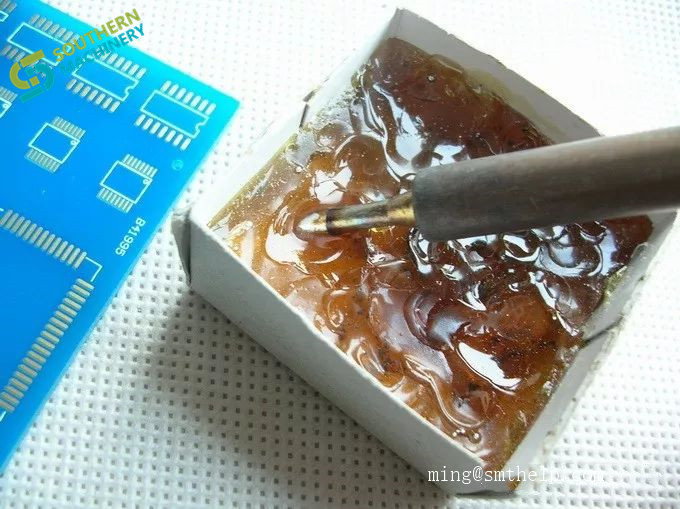
Solder paste collapse: collapse
the reason:
1. Low solder paste viscosity and poor thixotropy;
2. The high ambient temperature causes the viscosity to decrease naturally.
Solution for collapse:
1. Choose the right solder paste;
2. Control the ambient temperature.

Low solder tin: The solder at the solder joint is less than the required amount, which causes one or more parts of the welded part to not be completely covered by solder, or the lack of solder between the solder joints.
the reason:
1. The solder paste is not enough;
2. Poor solderability of pads and components;
3. Less reflow time;
4. Improper hole design;
5. The hole is blocked.
solution:
1. Thicken the missing version and increase the scraper pressure;
2. Improve solderability;
3. Increase the reflow time;
4. The smooth hole wall is easy to release solder paste and not easy to cause blockage;
5. (1) The solder paste removed from the refrigerator must be thawed (2) Check whether the solder paste has expired, (3) Avoid the solder paste staying on the template for too long, (4) Avoid printing under high humidity conditions.

More solder tin: The solder at the soldering place is much more than the normal demand, which makes it impossible to see the outline of the welded part or the solder to form a piled ball.

the reason:
1. The opening of the leaky version is too large;
2. The viscosity of solder paste is small.
solution:
1. Reduce the opening of the leaked version;
2. Increase the viscosity of solder paste.

Pointing: There is solder that protrudes outward in the form of needles or thorns, but there is no electrical short circuit formed by connection or contact with other places that should not be interconnected (such as pads or wires, etc.), also called burrs and drag tail.

the reason:
1. No wiping steel mesh or wiping frequency is not enough;
2. Equipment problems, no water spray, steel mesh paper can not wipe the steel mesh;
3. Repair welding occurs.
solution:
1. Standardize the wiping frequency of the tin printing machine (generally set to 5-6 boards for a wiping cycle);
2. Adjust the equipment to a normal level;
3. Training the skills of repair welders.

Holes: Various gases in the solder are improperly or poorly discharged during soldering. After cooling, holes of various shapes are formed on the surface or inside.

Cause: During the reflow, it is caused by the outgassing of the flux trapped in the solder joint.
solution:
1. Improve the solderability of components / substrates;
2. Use flux with high activity;
3. Reduce solder powder oxide;
4. Use inert heating gas;
5. The smallest component coverage area;
6. Separate molten solder joints during welding;
7. Slow down the preheating phase before reflow to promote soldering, and use the appropriate time at peak temperature.

Desoldering: also called open welding, open circuit; the pins / solder ends of the components are all detached or deviated from their corresponding pads, and the proper welding is not performed.

the reason:
1. Along with the tombstone and fierce wicking;
2. Lifting of components and PCB.
solution:
1. Use a solution to the tombstone;
2. Strengthen the rigidity of components through packaging design to avoid local heating.

Solder joint peeling: the pins of the welded components at the welding place

Solder joint stripping: The pin / weld electrode plating of the soldered component at the soldering site is separated from its body, or the soldered pad is stripped from the substrate.
Reason: due to the shrinkage stress of solder during cooling, reduce the amount of solder appropriately.
solution:
1. Improve PCB quality;
2. Reduce the amount of solder;
3. The slope of cooling.

Turned parts: The components are turned 180 degrees, according to IPC-A-610D welding standard capacitance resistance turned parts are acceptable (of course, some customer special requirements are not accepted, subject to customer requirements), other types of turned parts are not acceptable.
Reason: Bad feeder. The pressure of the feeder is too high. When the feeder is feeding, the thrust is too large, and the inertia acts, and the component rushes out of the turning piece and sucks.
solution:
1. Reduce Feida pressure;
2. The center of the material must correspond to the center of Feida.

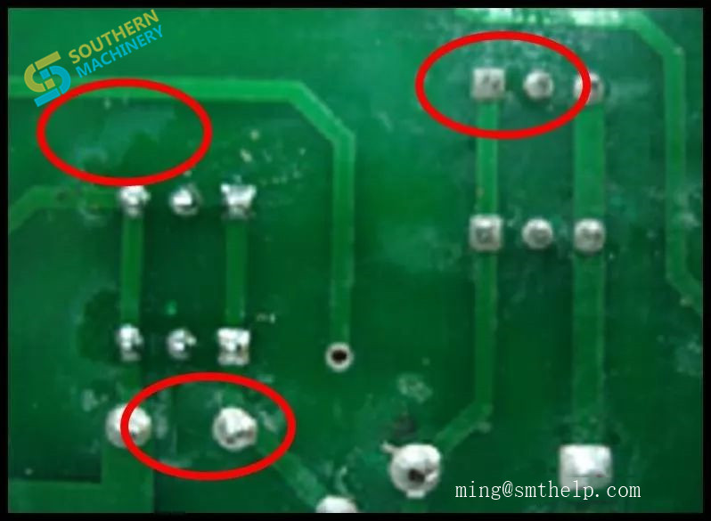
Flux residue: white spots (the flux residue that remains on the printed board after solder cleaning, white, yellow, gray or brown) and carbonized residue (caused by excessive heating)
the reason:
1. Avoid excessive heating and flux problems in solder paste;
2. Avoid excessive heating and prevent oxidation.
solution:
1.1 Use flux with thermally stable ingredients;
1.2 Flux using anti-oxidation stable ingredients;
1.3 Use flux that does not form insoluble metal salts;
1.4 Use properly cured solder mask and laminated PCB;
1.5 Cleaning agent with proper dissolving ability for flux residue;
1.6 Use a lower reflow temperature;
1.7 Use a shorter reflow time;
1.8 Use mechanical agitation when cleaning;
1.9 Use appropriate cleaning temperature;
2.1 Use flux with thermally stable ingredients;
2.2 Flux using anti-oxidation stable ingredients;
2.3 Use a lower reflow temperature;
2.4 Use shorter reflow time;
2.5 Use inert reflow gas.
3.If the residue is cleaned after reflow, the following three solutions will help alleviate the symptoms of carbonized residue:
(1) Use appropriate solvent cleaning agent to clean the flux residue;
(2) Use mechanical agitation when cleaning (use ultrasonic agitation or use higher spray pressure for cleaning);
(3) Adopt proper cleaning temperature (experiments have been made, black spots can be seen when manually washing with water at 77 ℃, no black spots can be seen when cleaning the components with room temperature water)

Solder cracks: There are visible or invisible fine cracks on the surface or inside of the solder at the solder joint.

the reason:
1. The top of the machine is broken;
2. Turnover storage.
solution:
1. Draw the position map of the thimble when connecting to prevent the component from being damaged;
2. The correct turnover storage method.

Automotive electronics PCB PCBA cleaning method, cleaning process, PCBA cleaning machine, flux cleaning (1)_副本

SMT small company survival magic weapon! Multi frequency, small batch,flexibility

SMT (Surface Mount Technology), or surface mount technology, is one of the most popular technologies and processes in the electronics assembly industry. In the Pearl River Delta represented by Shenzhen, the electronics and information industry is developed and the industry chain is complete. It is a veritable factory in the world.

Automotive electronics PCB PCBA cleaning method, cleaning process, PCBA cleaning machine, flux cleaning (1)_副本

As the market environment changes and technology changes, in order to meet the increasingly personalized needs of end customers, manufacturers are constantly improving their products, constantly innovating according to market needs, and developing trendy styles and functions to adapt to the current market demand. In order to be able to quickly respond to market diversified and uncertain needs and quickly provide products that meet customer needs, “short, flat, and fast” has become an important feature of production sites during this period, on time, quality, quantity and at a minimum cost Manufacturing products that meet customer needs has become the goal of production management, but progress is seemingly more and more difficult due to resource constraints such as limited skilled personnel and tight equipment. In this case, SMT production is now in a state of small batches and multiple varieties. Because of the inherent production characteristics of the SMT production line, it uses the best production efficiency in large batches. Therefore, for small batches and multiple varieties, there are multiple line changes to complete the production conversion of the product. The SMT line is in an intermittent production state. The increase has caused problems in the production efficiency of the SMT line.

One
Benefits of small batches and multiple varieties

1.Improve adaptability to changes in demand
Small batch, single piece delivery
Reduce job preparation time
Multi-skilled employees
In-process quality assurance system
Generalization of equipment and tooling

  1. Make manufacturing issues and their weaknesses visible
    Quality failure
    Equipment failure
    Workload imbalance
    Turnover time
  2. Eliminate waste caused by improper production management and reduce production management costs
    Material waiting due to improper production management
    Unnecessary model changes due to improper production management
    Increase in indirect operations due to improper production management

4.Improve the adaptability of manufacturing to short delivery time
Eliminate stagnation (things / information)
Reduce the number of intermediate work in process
Synchronization

two
Characteristics of small batches and multiple varieties

Multi-variety parallel

Because many enterprises’ products are configured for customers, different products have different needs, and the resources of enterprises are among multiple varieties.

Resource sharing
Every task in the production process requires resources, but the resources that can be used in the actual process are very limited. For example, the problem of equipment conflicts often encountered in the production process is caused by the sharing of project resources. Therefore, limited resources must be properly allocated to meet project needs.

  1. Uncertainty of order result and production cycle
    Due to the instability of customer needs, the clearly defined nodes are inconsistent with the complete cycle of human, machine, material, method, ring, etc., the production cycle is often uncertain, and projects with insufficient cycles require more resources. , Increasing the difficulty of production control.
  • Material requirements change, resulting in serious procurement delays
    Due to the insertion or change of orders, it is difficult for external processing and procurement to reflect the order delivery time. Supply risks are extremely high due to small quantities and a single source of supply.

  • three
    Difficulties in small batch and multi-variety production

    1. Dynamic process path planning and deployment of virtual unit lines: emergency insertion, equipment failure, and bottleneck drift.
    2. Identification and drift of bottlenecks: before and during production
    3. Multi-level bottlenecks: bottlenecks on assembly lines, bottlenecks on virtual lines of parts, how to coordinate and couple.
    4. Buffer size: either backlog or poor interference resistance. Production batch, transfer batch, etc.
    5. Production scheduling: not only consider bottlenecks, but also the impact of non-bottleneck resources.

    Many varieties and small batch production models will also encounter many problems in enterprise practice, such as:
    Multi-variety and low-batch production, mixed scheduling is difficult
    Unable to deliver on time, too much “fire fighting” overtime
    Order requires too much follow-up
    Frequent changes in production priorities, the original plan could not be implemented
    Increasing inventory but often lacking critical materials
    The production cycle is too long, the lead time is infinitely expanded

    ▎How to implement automatic upgrade has become a trouble for OEM companies

    The electronic information industry is still a pillar industry in Shenzhen, with an industrial scale of more than 1.200 billion yuan, accounting for about 1/7 of the national electronic information manufacturing revenue. In Shenzhen, there are a large number of leading electronic information companies such as Huawei, ZTE, and TCL, as well as a large number of small-scale lean manufacturing and processing enterprises that were born in response to the needs of the times.

    Due to the production characteristics of traditional foundry companies, “different bills of materials for each order, different production processes, different cleaning standards, different packaging requirements, and different labeling specifications”, unlike large factories that do standard products, they can be automated on a large scale upgrade.

    How to use industrial robots, advanced automation management platforms, and information technology to help these enterprises achieve flexible production and agile manufacturing are the topics they care about in common.

    Under the pressure, many traditional OEM companies have begun to transform to ODM (Original Design Manufacturer), and gradually pay attention to independent intellectual property rights, start to make innovative products, and start to develop independent brands.

    ▎ Machine substitution may be a “beautiful trap”, how to realize flexible production is the key

    China’s Industry 4.0, like an aircraft carrier, propels China forward. For these small and small batch OEM companies, after experiencing the “prosperity era” brought by the demographic dividend, they are also thinking about how to take the road of independent innovation.

    Perhaps many OEM companies rely on the channel advantages accumulated over many years of operation and the natural industrial chain advantages of the Pearl River Delta. But the demographic dividend is no longer, the cost advantage is no longer, and the rise and penetration of the Internet has also led to major changes in production methods, management concepts, production equipment, and even raw materials. These factors have begun to cause some entrepreneurs to worry about the future.

    “Without the independent innovation of Chinese companies, we can only be a world factory. Without trial and error and iteration of research and development, we will never have our own core technology.”

    How to innovate? Is machine substitution really the general trend?

    For these manufacturers, there may be pitfalls in purely pursuing “machine substitution” oriented by automated equipment, mass production, and reduced manufacturing costs. Because for them, the key to “machine substitution” is how to implement software flexibility, agile programming, or automatic programming, just like “quick mode change” in TPS (transaction processing system).

    Automotive electronics PCB PCBA cleaning method, cleaning process, PCBA cleaning machine, flux cleaning

    How to distinguish between PCBA board cleaning and non-washing in automotive electronics?

    How to distinguish between PCBA board cleaning and non-washing in automotive electronics?

    Edited by Ming: ming@smthelp.net

    Customers often do not understand why automotive electronics PCBA boards need to be cleaned reliably. Which electronic PCBAs need cleaning before use? Which ones don’t have to be cleaned? It is also difficult to distinguish and judge. The purpose of this article is to analyze the necessary reliability cleaning of automotive electronics PCBA, hoping to help customers and readers.

    Automotive electronics PCB PCBA cleaning method, cleaning process, PCBA cleaning machine, flux cleaning
    Automotive electronics PCB PCBA cleaning method, cleaning process, PCBA cleaning machine, flux cleaning

    Automotive electronics PCB PCBA cleaning method, cleaning process, PCBA cleaning machine, flux cleaning
    Automotive electronics PCB PCBA cleaning method, cleaning process, PCBA cleaning machine, flux cleaning

    In order to realize the control of driving and clock functions in the car, various types of electronic circuit boards are used to realize various control functions: engine driving management system or engine driving computer ECU, and new energy vehicles have more circuit boards, each of which is on average. The car has a circuit area of ​​1.5 square meters and more than 100 electronic circuit boards. These types are in electronic circuit boards that implement various functions. What needs cleaning? Which do not have to be cleaned?

    Automotive electronics PCB PCBA cleaning method, cleaning process, PCBA cleaning machine, flux cleaning
    Automotive electronics PCB PCBA cleaning method, cleaning process, PCBA cleaning machine, flux cleaning

    The function control panel of the car electronics is cleaned and not cleaned, and is often distinguished from the driver’s personal safety, the safety of the driving scene and the safety of the property. The function control related to the safety of the car and the personal safety of the third party is required. Do the cleaning to achieve high reliability technical requirements: for example, the engine management system ECU circuit board, the new energy vehicle power management system BMS circuit board and so on.

    Automotive electronics PCB PCBA cleaning method, cleaning process, PCBA cleaning machine, flux cleaning
    Automotive electronics PCB PCBA cleaning method, cleaning process, PCBA cleaning machine, flux cleaning

    The car also has other management systems, lighting control systems, navigation, music playback entertainment systems, door and window control and glass lift, seat functions and other auxiliary functions, because the density of these systems and human life safety is not too great, Often such electronic circuit boards can be made from no-clean, thereby reducing cost and meeting performance requirements.

    Automotive electronics PCB PCBA cleaning method, cleaning process, PCBA cleaning machine, flux cleaning (1)_副本
    Automotive electronics PCB PCBA cleaning method, cleaning process, PCBA cleaning machine, flux cleaning

    Driving circuit ECU, new energy vehicle BMS power management system process circuit board process cleaning, cleaning circuit board surface residue, removing flux, solder paste residue and residual effects of other pollutants in the process, truly reach the circuit The surface of the board assembly is clean, and the degree of ionic contamination is used as an indicator to measure the cleanliness of the board surface. This is the technical indicator that can truly achieve reliability guarantee. It can greatly improve the safety and reliability of the circuit board assembly products, and avoid unnecessary risks caused by the electrochemical corrosion of the circuit board and the defects caused by electromigration caused by poor working conditions, humidity and high temperature.

    In summary, all component processes that are closely related to life safety and driving safety must be reliably cleaned. It is currently recommended to use an environmentally safe water-based cleaning process.

    SMTHELP :SMT Professional Manufacturer PCB Cleaning Machine
    The product is suitable for use in automotive electronics, smart home products, communications electronics, consumer electronic product manufacturing process, to improve product reliability and to remove foreign bodies and electrostatic PCB surface
    PCB cleaner,nozzle cleaning machine,PCB Stencil cleaning machine, PCBA cleaning machine,Fixture cleaning machine,Printer Cleaning Machine,pneumatic Stencil cleaning machine,fully pneumatic washing machine Manufacturer

    https://www.smthelp.net/pcb-cleaning-machine/

    https://www.smthelp.net/scm5600d-pcba-cleaning-machine/

    PCBA CLEANING MACHINE SCM5600D (2)
    PCBA CLEANING MACHINE SCM5600D (2

    PCBA cleaning method, cleaning process, PCBA cleaning machine, flux cleaning (1)

    Circuit board, PCBA cleaning is really important for EMS (Electronic Manufacturing Service)?

    Circuit board, PCBA cleaning, is it really important for EMS (Electronic Manufacturing Service)?

    Edited by Ming: ming@smthelp.net

    “Cleaning” is often overlooked during board (PCB) PCBA manufacturing and is considered to be not a critical step. However, with the long-term use of the product on the client side, the problems caused by the ineffective cleaning in the early stage caused many failures, and the rework or recall of the product caused a sharp increase in operating costs. Below, SMTHELP briefly explains the role of PCBA cleaning of circuit boards (circuit boards).

    PCBA cleaning method, cleaning process, PCBA cleaning machine, flux cleaning (1)
    PCBA cleaning method, cleaning process, PCBA cleaning machine, flux cleaning (1)

    PC BA (Printed Circuit Assembly) has a number of process stages in the production process, each stage is contaminated to varying degrees, so the surface of the PCBA of the circuit board (circuit board) is left with various deposits or impurities, which will lower the product. Performance, and even cause product failure. For example, in the process of soldering electronic components, solder paste, flux, etc. are used for auxiliary soldering, and residues are generated after soldering, and the residue contains organic acids and ions, etc., in which organic acids corrode the circuit board (circuit board) PCBA, and The presence of electrical ions can cause short circuits and cause product failure.

    PCBA cleaning method, cleaning process, PCBA cleaning machine, flux cleaning (1)
    PCBA cleaning method, cleaning process, PCBA cleaning machine, flux cleaning (1)

    There are many kinds of contaminants on PCB (PCB) PCBA, which can be classified into two types: ionic and non-ionic. The ionic pollutants are exposed to moisture in the environment, and electrochemical migration occurs after energization, forming a dendritic structure, resulting in a low resistance path and destroying the PCBA function of the circuit board (circuit board). Non-ionic contaminants can penetrate the insulating layer of PC B and grow dendrites under the surface of the PCB. In addition to ionic and non-ionic contaminants, there are also particulate contaminants such as solder balls, floating spots in solder baths, dust, dust, etc. These contaminants can lead to reduced solder joint quality, sharp solder joints during soldering, and Porosity, short circuit and many other undesirable phenomena.


    With so many pollutants, which ones are the most concerned? Fluxes or solder pastes are commonly used in reflow and wave soldering processes. They are mainly composed of solvents, wetting agents, resins, corrosion inhibitors and activators. Thermally modified products must be present after soldering. In all the pollutants, the post-weld residue is the most important factor affecting the quality of the product. The ionic residue tends to cause electromigration to reduce the insulation resistance, and the rosin resin residue is easy to adsorb. Dust or impurities cause an increase in contact resistance, and in severe cases, open circuit failure, so strict cleaning must be performed after welding to ensure the quality of PCBA of the circuit board (circuit board).

    PCBA cleaning method, cleaning process, PCBA cleaning machine, flux cleaning (1)
    PCBA cleaning method, cleaning process, PCBA cleaning machine, flux cleaning (1)

    In summary, the cleaning of the circuit board (PCB) PCBA is very important, and “cleaning” is an important process that is directly related to the quality of the PCB (circuit board) PCBA, which is indispensable.

    PCBA cleaning method, cleaning process, PCBA cleaning machine, flux cleaning (1)
    PCBA cleaning method, cleaning process, PCBA cleaning machine, flux cleaning (1)

    Circuit board, PCBA cleaning is really important, for EMS (Electronic Manufacturing Service)?

    SMTHELP :SMT Professional Manufacturer PCB Cleaning Machine
    The product is suitable for use in automotive electronics, smart home products, communications electronics, consumer electronic product manufacturing process, to improve product reliability and to remove foreign bodies and electrostatic PCB surface
    PCB cleaner,nozzle cleaning machine,PCB Stencil cleaning machine, PCBA cleaning machine,Fixture cleaning machine,Printer Cleaning Machine,pneumatic Stencil cleaning machine,fully pneumatic washing machine Manufacturer

    https://www.smthelp.net/pcb-cleaning-machine/

    https://www.smthelp.net/scm5600d-pcba-cleaning-machine/

    PCBA CLEANING MACHINE SCM5600D (2)
    PCBA CLEANING MACHINE SCM5600D (2

    PCBA cleaning method, cleaning process, PCBA cleaning machine, flux cleaning (1)

    After the PCBA is cleaned, the board surface turns white, what should we do?

    After the circuit board is cleaned, the board surface turns white, what should we do?

    Edited by Ming: ming@smthelp.net

    First, the board surface is whitish after cleaning:

    In the electronic component manufacturing process, the PCBA circuit board is often over-wave soldered, and after the manual cleaning agent is used for cleaning, the board surface appears white (Figure 1).

    PCBA cleaning method, cleaning process, PCBA cleaning machine, flux cleaning (1)
    PCBA cleaning method, cleaning process, PCBA cleaning machine, flux cleaning (1)

    Figure 1
    After the cleaning of the PCBA solder joints, the white surface of the board surface appears after being placed, and the white mark is scattered around the solder joints, which seriously affects the appearance acceptance.

    Second, the reason for the whitish surface of the board after cleaning:

    White residue is a common contaminant on PCBA and is generally a by-product of flux. Common white residues are polymerized rosin, unreacted activator, and lead metal chloride or bromide, which react with flux and solder. These substances expand in volume after moisture absorption, and some substances also hydrate with water. White residue is becoming more and more obvious. It is extremely difficult to remove these residues on the PCB. If the temperature is too hot or high, the problem is more serious. The infrared spectroscopy analysis of the rosin and residue on the PCB surface before and after the soldering process confirms the process. .

    PCBA cleaning method, cleaning process, PCBA cleaning machine, flux cleaning (1)
    PCBA cleaning method, cleaning process, PCBA cleaning machine, flux cleaning (1)

    Regardless of whether the board has white residue after cleaning, or if the white material appears after the no-clean circuit board is stored, or the white substance on the solder joint found during the repair, there are four cases:

    1. Rosin in the flux: Most of the white matter produced after the cleaning is not clean, stored, and the solder joint fails, is the inherent rosin in the flux. Rosin is usually a transparent, hard and brittle solid material with no fixed shape, not a crystal. Rosin is thermodynamically unstable and has a tendency to crystallize. After the rosin crystallizes, the colorless transparent body becomes a white powder. If the cleaning is not clean, the white residue may be a crystalline powder formed by the rosin after the solvent is volatilized.

    When the PCB is stored under high humidity conditions, when the absorbed moisture reaches a certain level, the rosin gradually changes from a colorless and transparent glass state to a crystalline state, and a white powder is formed from a viewing angle.

    PCBA cleaning method, cleaning process, PCBA cleaning machine, flux cleaning (1)
    PCBA cleaning method, cleaning process, PCBA cleaning machine, flux cleaning (1)

    The essence is still rosin, but the shape is different, still has good insulation, and will not affect the performance of the board. The abietic acid and halide (if used) in the rosin are used together as an active agent. Synthetic resins generally do not react with metal oxides below 100 ° C, but react rapidly when the temperature is higher than 100 ° C. They volatilize and decompose faster, and have low solubility in water.

    1. Rosin denature: This is the substance produced by the reaction of rosin and flux during the welding process, and the solubility of this material is generally poor, it is not easy to be cleaned, and it stays on the board to form a white residue. But these white substances are all organic, still guarantee the reliability of the board.
    2. Organometallic salt: The principle of removing the oxide of the welding surface is that the organic acid reacts with the metal oxide to form a metal salt soluble in liquid rosin. After cooling, it forms a solid solution with the rosin, and is removed together with the rosin in the cleaning.

    If the welding surface and parts are highly oxidized, the concentration of the product after welding will be high. When the degree of oxidation of the rosin is too high, it may remain on the board together with the undissolved rosin oxide. At this time, the reliability of the board will be reduced.

    1. Metallic inorganic salts: These may be metal oxides in solders and halogen-containing active agents in flux or solder paste, halide ions in PCB pads, halide ion residues in the surface coating of components, halogen-containing materials in FR4 materials. The substance formed by the reaction of the halide ion released at a high temperature generally has a small solubility in an organic solvent.

    PCBA cleaning method, cleaning process, PCBA cleaning machine, flux cleaning (1)
    PCBA cleaning method, cleaning process, PCBA cleaning machine, flux cleaning (1)

    In the assembly process, it is highly probable that the halogen-containing flux is used for the electronic auxiliary materials (although the supplier provides environmentally friendly flux, but the halogen-free flux is still relatively small), and the surface of the board remains after welding. Halogen-based ions (F, Cl, Br, l). These ionic halogen residues, which are not themselves white, are not sufficient to cause whitening of the surface. These substances form strong acids when exposed to water or moisture. These strong acids begin to react with the oxide layer on the surface of the solder joints to form acid salts, which are white substances that are seen.

    Third, after the circuit board is cleaned, the board surface is whitened:

    1, the general solution:

    1. Washing method Note: When washing the PCB, the PCBA should be tilted. Do not lay it flat. You can place the paper in the washing station, so that most of the washed solution will flow down;
  • Do not wash the plate repeatedly for repeated times, and increase the frequency of replacement depending on the situation;
  • 3, and then start from the washing water formula, you can ask the supplier to improve the formula, improve the cleaning degree and dissolution volatility.

    1. How to completely solve the problem of whitening of the board after cleaning the circuit board?

    For the whitening problem of PCBA circuit board cleaning, water-based cleaning agent can be used to meet the corresponding cleaning equipment to deal with it. It is safe and environmentally friendly, meets the requirements of current ROHS, CE, and other environmental protection regulations. It has high cleaning efficiency and completely solves the problem of whitening.

    SMTHELP :SMT Professional Manufacturer PCB Cleaning Machine
    The product is suitable for use in automotive electronics, smart home products, communications electronics, consumer electronic product manufacturing process, to improve product reliability and to remove foreign bodies and electrostatic PCB surface
    PCB cleaner,nozzle cleaning machine,PCB Stencil cleaning machine, Printer Cleaning Machine,pneumatic Stencil cleaning machine,fully pneumatic washing machine Manufacturer

    https://www.smthelp.net/pcb-cleaning-machine/

    https://www.smthelp.net/scm5600d-pcba-cleaning-machine/

    PCBA CLEANING MACHINE SCM5600D (2)
    PCBA CLEANING MACHINE SCM5600D (2)

    3D showing SMT nozzle for EMS factory