We specialize in Auto Insertion machine and SMT equipments, provide spare parts, sub-assembly, retrofit kit, repair kit, upgrading, training, overhaul service, quality problem free replacement.And we will provide customers with high quality after-sales service, free technical support etc, welcome inquiry: info@smthelp.net
[embeddoc url=”https://www.smthelp.net/wp-content/uploads/2020/05/SMT-stencil-laser-making-machine.pdf” download=”all”]SMT stencil production process (reference)
General technical requirements:
1. Screen frame: The frame size is determined according to the requirements of the printing machine. Taking DEK265 and MPM UP 3000 as an example, the frame size is 29ˊ
29ˊ, using aluminum alloy, frame profile specification is 1.5ˊ 1.5ˊ.
Stretching the net: Adopt the red glue + aluminum tape method, at the junction of the aluminum frame and the glue, a layer of protective paint must be evenly scraped. At the same time, in order to ensure that the screen has sufficient tension and good flatness, it is recommended that the stainless steel plate be kept 25mm-50mm away from the inside of the screen frame.
Reference point: According to the size and shape provided by the PCB information, the opening is 1: 1, and the translucent is engraved on the reverse side of the printing. At the corresponding coordinates, the entire PCB opens at least two reference points.
Opening requirements: 1.41. The position and size ensure a high opening accuracy, and the opening is strictly in accordance with the prescribed opening method. 1.42. The size of the independent opening cannot be too large, the width cannot be greater than 2mm, and a 0.4mm bridge is required in the middle of the pad size greater than 2mm, so as not to affect the strength of the stencil.
1.43. The opening area must be centered.
Characters: In order to facilitate production, it is recommended to engrave the following characters in the lower left or lower right corner of the screen: Model; T; Date; the name of the company that made the screen.
Stencil thickness: In order to ensure the amount of solder paste printing and welding quality, the surface of the stencil is smooth and even, and the thickness is uniform. The stencil thickness refers to the above table. The stencil thickness should meet the premise of the finest pitch QFP BGA. If there are 0.5mmQFP and CHIP 0402 components on the PCB, the stencil thickness is 0.12mm; if there are 0.5mmQFP and CHIP 0603 or more components on the PCB, the stencil thickness is 0.15mm;
The opening shape and size requirements of printed tin screen:
General principle: According to the requirements of the IPC-7525 steel mesh design guide, in order to ensure that the solder paste can be smoothly released from the opening of the stencil to the PCB pad, in the opening of the stencil to view polyester 1. The area ratio / width-to-thickness ratio area ratio is greater than 0.66 2. The mesh hole wall is smooth. Especially for QFP and CSP with a pitch of less than 0.5mm, suppliers are required to perform electro-polishing during the manufacturing process. 3.) With the printing surface as the upper side, the lower opening of the mesh opening should be 0.01mm or 0.02mm wider than the upper opening, that is, the opening is inverted tapered, which facilitates the ineffective release of solder paste and reduces the number of times of cleaning the stencil. Normally, the size and shape of the opening of the SMT element is the same as the pad, and the opening is 1: 1. Under special circumstances, for some special SMT components, the size and shape of the screen openings are specified.
No. 2 Special SMT component screen opening:
2.1CHIP components: CHIP components above 0603, in order to effectively prevent the generation of tin beads.
2.2SOT89 components: Due to the large pad and small pad spacing between components, soldering quality problems such as tin beads are prone to occur.
2.3 SOT252 component: Because SOT252 has a large pad, it is easy to produce tin beads, and the reflow soldering tension causes displacement.
Look 2.4IC: A. For the standard pad design, PITCH》 = 0.65mm IC, the opening width is 90% of the pad width, and the length is unchanged.
B. For the standard pad design, IC with PITCH <= 005mm, because of its small PITCH, it is easy to produce bridging, the length direction of the steel mesh opening is unchanged, the opening width is 0.5PITCH, and the opening width is 0.25mm.
2.5 Other situations: One pad is too large, usually one side is greater than 4mm, and the other side is not less than 2.5mm, in order to prevent the generation of tin beads and displacement caused by the effect of tension, the mesh opening is recommended to be divided by grid lines In this way, the grid line width is 0.5mm and the grid size is 2mm, which can be evenly divided according to the pad size.
The shape and size requirements of the opening of the printed rubber screen: glue is used for simple PCB assembly. Dispensing is preferred. CHIP, MELF, SOT components are printed through the screen, and IC is used to avoid glue scraping. Here, only the recommended opening size and opening shape of CHIP, MELF and SOT offset printing plates are given.
1. Two diagonal positioning holes must be opened at the diagonal of the stencil. Select FIDUCIAL MARK to open the hole.
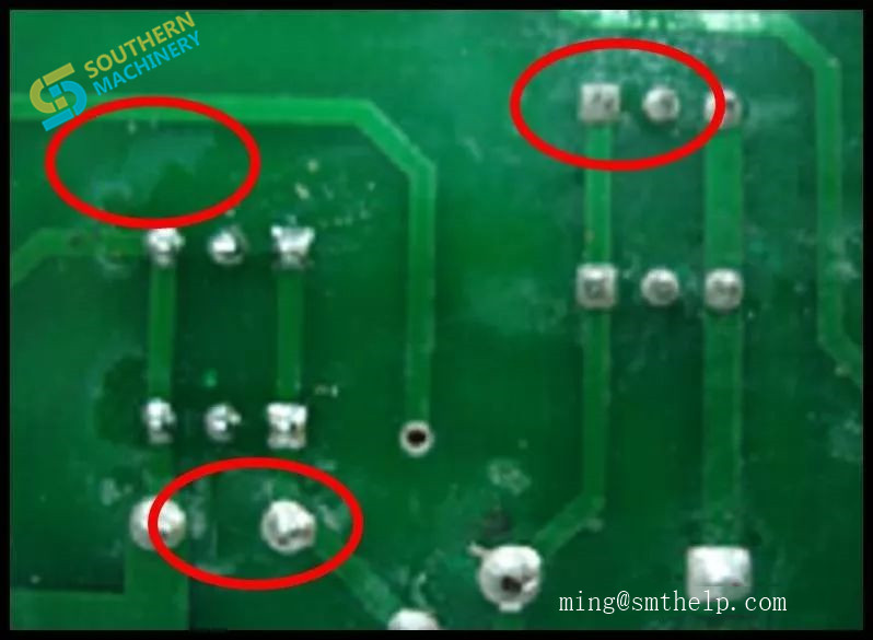
The openings are all elongated. Inspection method 1) Visually check that the opening is centered and the net is flat. 2) Check the correctness of the stencil opening through the PCB entity. 3) Examine the length and width of the screen opening and the smoothness of the hole wall and the surface of the steel sheet with a scaled high power microscope. 4) The thickness of the steel sheet is verified by detecting the thickness of the solder paste after printing tin, that is, the result verification. Conclusion The technical requirements for screen design have been tested for a period of time, and the print quality has been well controlled. The PPM of SMT welding quality has dropped from about 1300ppm to about 130ppm. Due to the development of the packaging direction of modern electronic components, higher requirements have also been placed on the design of steel mesh. Is a subject that we need to focus on in the future
SMT (Surface Mount Technology), or surface mount technology, is one of the most popular technologies and processes in the electronics assembly industry. In the Pearl River Delta represented by Shenzhen, the electronics and information industry is developed and the industry chain is complete. It is a veritable factory in the world.
As the market environment changes and technology changes, in order to meet the increasingly personalized needs of end customers, manufacturers are constantly improving their products, constantly innovating according to market needs, and developing trendy styles and functions to adapt to the current market demand. In order to be able to quickly respond to market diversified and uncertain needs and quickly provide products that meet customer needs, “short, flat, and fast” has become an important feature of production sites during this period, on time, quality, quantity and at a minimum cost Manufacturing products that meet customer needs has become the goal of production management, but progress is seemingly more and more difficult due to resource constraints such as limited skilled personnel and tight equipment. In this case, SMT production is now in a state of small batches and multiple varieties. Because of the inherent production characteristics of the SMT production line, it uses the best production efficiency in large batches. Therefore, for small batches and multiple varieties, there are multiple line changes to complete the production conversion of the product. The SMT line is in an intermittent production state. The increase has caused problems in the production efficiency of the SMT line.
One
Benefits of small batches and multiple varieties
1.Improve adaptability to changes in demand
Small batch, single piece delivery
Reduce job preparation time
Multi-skilled employees
In-process quality assurance system
Generalization of equipment and tooling
Make manufacturing issues and their weaknesses visible
Quality failure
Equipment failure
Workload imbalance
Turnover time
Eliminate waste caused by improper production management and reduce production management costs
Material waiting due to improper production management
Unnecessary model changes due to improper production management
Increase in indirect operations due to improper production management
4.Improve the adaptability of manufacturing to short delivery time
Eliminate stagnation (things / information)
Reduce the number of intermediate work in process
Synchronization
two
Characteristics of small batches and multiple varieties
Multi-variety parallel
Because many enterprises’ products are configured for customers, different products have different needs, and the resources of enterprises are among multiple varieties.
Resource sharing
Every task in the production process requires resources, but the resources that can be used in the actual process are very limited. For example, the problem of equipment conflicts often encountered in the production process is caused by the sharing of project resources. Therefore, limited resources must be properly allocated to meet project needs.
Uncertainty of order result and production cycle
Due to the instability of customer needs, the clearly defined nodes are inconsistent with the complete cycle of human, machine, material, method, ring, etc., the production cycle is often uncertain, and projects with insufficient cycles require more resources. , Increasing the difficulty of production control.
Material requirements change, resulting in serious procurement delays
Due to the insertion or change of orders, it is difficult for external processing and procurement to reflect the order delivery time. Supply risks are extremely high due to small quantities and a single source of supply.
three
Difficulties in small batch and multi-variety production
Dynamic process path planning and deployment of virtual unit lines: emergency insertion, equipment failure, and bottleneck drift.
Identification and drift of bottlenecks: before and during production
Multi-level bottlenecks: bottlenecks on assembly lines, bottlenecks on virtual lines of parts, how to coordinate and couple.
Buffer size: either backlog or poor interference resistance. Production batch, transfer batch, etc.
Production scheduling: not only consider bottlenecks, but also the impact of non-bottleneck resources.
Many varieties and small batch production models will also encounter many problems in enterprise practice, such as:
Multi-variety and low-batch production, mixed scheduling is difficult
Unable to deliver on time, too much “fire fighting” overtime
Order requires too much follow-up
Frequent changes in production priorities, the original plan could not be implemented
Increasing inventory but often lacking critical materials
The production cycle is too long, the lead time is infinitely expanded
▎How to implement automatic upgrade has become a trouble for OEM companies
The electronic information industry is still a pillar industry in Shenzhen, with an industrial scale of more than 1.200 billion yuan, accounting for about 1/7 of the national electronic information manufacturing revenue. In Shenzhen, there are a large number of leading electronic information companies such as Huawei, ZTE, and TCL, as well as a large number of small-scale lean manufacturing and processing enterprises that were born in response to the needs of the times.
Due to the production characteristics of traditional foundry companies, “different bills of materials for each order, different production processes, different cleaning standards, different packaging requirements, and different labeling specifications”, unlike large factories that do standard products, they can be automated on a large scale upgrade.
How to use industrial robots, advanced automation management platforms, and information technology to help these enterprises achieve flexible production and agile manufacturing are the topics they care about in common.
Under the pressure, many traditional OEM companies have begun to transform to ODM (Original Design Manufacturer), and gradually pay attention to independent intellectual property rights, start to make innovative products, and start to develop independent brands.
▎ Machine substitution may be a “beautiful trap”, how to realize flexible production is the key
China’s Industry 4.0, like an aircraft carrier, propels China forward. For these small and small batch OEM companies, after experiencing the “prosperity era” brought by the demographic dividend, they are also thinking about how to take the road of independent innovation.
Perhaps many OEM companies rely on the channel advantages accumulated over many years of operation and the natural industrial chain advantages of the Pearl River Delta. But the demographic dividend is no longer, the cost advantage is no longer, and the rise and penetration of the Internet has also led to major changes in production methods, management concepts, production equipment, and even raw materials. These factors have begun to cause some entrepreneurs to worry about the future.
“Without the independent innovation of Chinese companies, we can only be a world factory. Without trial and error and iteration of research and development, we will never have our own core technology.”
How to innovate? Is machine substitution really the general trend?
For these manufacturers, there may be pitfalls in purely pursuing “machine substitution” oriented by automated equipment, mass production, and reduced manufacturing costs. Because for them, the key to “machine substitution” is how to implement software flexibility, agile programming, or automatic programming, just like “quick mode change” in TPS (transaction processing system).
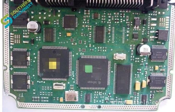
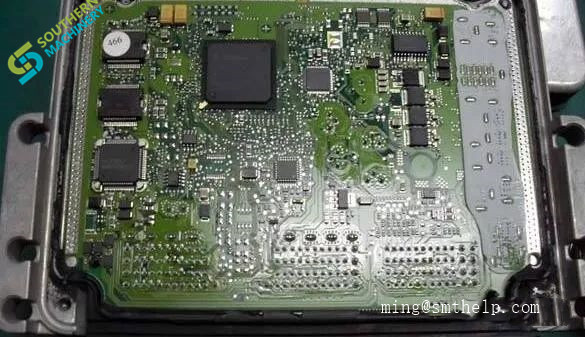
How to distinguish between PCBA board cleaning and non-washing in automotive electronics?
Edited by Ming: ming@smthelp.net
Customers often do not understand why automotive electronics PCBA boards need to be cleaned reliably. Which electronic PCBAs need cleaning before use? Which ones don’t have to be cleaned? It is also difficult to distinguish and judge. The purpose of this article is to analyze the necessary reliability cleaning of automotive electronics PCBA, hoping to help customers and readers.
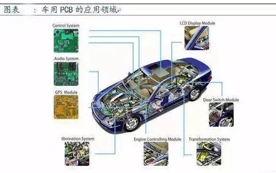
In order to realize the control of driving and clock functions in the car, various types of electronic circuit boards are used to realize various control functions: engine driving management system or engine driving computer ECU, and new energy vehicles have more circuit boards, each of which is on average. The car has a circuit area of 1.5 square meters and more than 100 electronic circuit boards. These types are in electronic circuit boards that implement various functions. What needs cleaning? Which do not have to be cleaned?
The function control panel of the car electronics is cleaned and not cleaned, and is often distinguished from the driver’s personal safety, the safety of the driving scene and the safety of the property. The function control related to the safety of the car and the personal safety of the third party is required. Do the cleaning to achieve high reliability technical requirements: for example, the engine management system ECU circuit board, the new energy vehicle power management system BMS circuit board and so on.
The car also has other management systems, lighting control systems, navigation, music playback entertainment systems, door and window control and glass lift, seat functions and other auxiliary functions, because the density of these systems and human life safety is not too great, Often such electronic circuit boards can be made from no-clean, thereby reducing cost and meeting performance requirements.
Driving circuit ECU, new energy vehicle BMS power management system process circuit board process cleaning, cleaning circuit board surface residue, removing flux, solder paste residue and residual effects of other pollutants in the process, truly reach the circuit The surface of the board assembly is clean, and the degree of ionic contamination is used as an indicator to measure the cleanliness of the board surface. This is the technical indicator that can truly achieve reliability guarantee. It can greatly improve the safety and reliability of the circuit board assembly products, and avoid unnecessary risks caused by the electrochemical corrosion of the circuit board and the defects caused by electromigration caused by poor working conditions, humidity and high temperature.
In summary, all component processes that are closely related to life safety and driving safety must be reliably cleaned. It is currently recommended to use an environmentally safe water-based cleaning process.
SMTHELP :SMT Professional Manufacturer PCB Cleaning Machine
The product is suitable for use in automotive electronics, smart home products, communications electronics, consumer electronic product manufacturing process, to improve product reliability and to remove foreign bodies and electrostatic PCB surface
PCB cleaner,nozzle cleaning machine,PCB Stencil cleaning machine, PCBA cleaning machine,Fixture cleaning machine,Printer Cleaning Machine,pneumatic Stencil cleaning machine,fully pneumatic washing machine Manufacturer
Circuit board, PCBA cleaning, is it really important for EMS (Electronic Manufacturing Service)?
Edited by Ming: ming@smthelp.net
“Cleaning” is often overlooked during board (PCB) PCBA manufacturing and is considered to be not a critical step. However, with the long-term use of the product on the client side, the problems caused by the ineffective cleaning in the early stage caused many failures, and the rework or recall of the product caused a sharp increase in operating costs. Below, SMTHELP briefly explains the role of PCBA cleaning of circuit boards (circuit boards).
PC BA (Printed Circuit Assembly) has a number of process stages in the production process, each stage is contaminated to varying degrees, so the surface of the PCBA of the circuit board (circuit board) is left with various deposits or impurities, which will lower the product. Performance, and even cause product failure. For example, in the process of soldering electronic components, solder paste, flux, etc. are used for auxiliary soldering, and residues are generated after soldering, and the residue contains organic acids and ions, etc., in which organic acids corrode the circuit board (circuit board) PCBA, and The presence of electrical ions can cause short circuits and cause product failure.
There are many kinds of contaminants on PCB (PCB) PCBA, which can be classified into two types: ionic and non-ionic. The ionic pollutants are exposed to moisture in the environment, and electrochemical migration occurs after energization, forming a dendritic structure, resulting in a low resistance path and destroying the PCBA function of the circuit board (circuit board). Non-ionic contaminants can penetrate the insulating layer of PC B and grow dendrites under the surface of the PCB. In addition to ionic and non-ionic contaminants, there are also particulate contaminants such as solder balls, floating spots in solder baths, dust, dust, etc. These contaminants can lead to reduced solder joint quality, sharp solder joints during soldering, and Porosity, short circuit and many other undesirable phenomena.
With so many pollutants, which ones are the most concerned? Fluxes or solder pastes are commonly used in reflow and wave soldering processes. They are mainly composed of solvents, wetting agents, resins, corrosion inhibitors and activators. Thermally modified products must be present after soldering. In all the pollutants, the post-weld residue is the most important factor affecting the quality of the product. The ionic residue tends to cause electromigration to reduce the insulation resistance, and the rosin resin residue is easy to adsorb. Dust or impurities cause an increase in contact resistance, and in severe cases, open circuit failure, so strict cleaning must be performed after welding to ensure the quality of PCBA of the circuit board (circuit board).
In summary, the cleaning of the circuit board (PCB) PCBA is very important, and “cleaning” is an important process that is directly related to the quality of the PCB (circuit board) PCBA, which is indispensable.
After the circuit board is cleaned, the board surface turns white, what should we do?
Edited by Ming: ming@smthelp.net
First, the board surface is whitish after cleaning:
In the electronic component manufacturing process, the PCBA circuit board is often over-wave soldered, and after the manual cleaning agent is used for cleaning, the board surface appears white (Figure 1).
After the cleaning of the PCBA solder joints, the white surface of the board surface appears after being placed, and the white mark is scattered around the solder joints, which seriously affects the appearance acceptance.
Second, the reason for the whitish surface of the board after cleaning:
White residue is a common contaminant on PCBA and is generally a by-product of flux. Common white residues are polymerized rosin, unreacted activator, and lead metal chloride or bromide, which react with flux and solder. These substances expand in volume after moisture absorption, and some substances also hydrate with water. White residue is becoming more and more obvious. It is extremely difficult to remove these residues on the PCB. If the temperature is too hot or high, the problem is more serious. The infrared spectroscopy analysis of the rosin and residue on the PCB surface before and after the soldering process confirms the process. .
Regardless of whether the board has white residue after cleaning, or if the white material appears after the no-clean circuit board is stored, or the white substance on the solder joint found during the repair, there are four cases:
Rosin in the flux: Most of the white matter produced after the cleaning is not clean, stored, and the solder joint fails, is the inherent rosin in the flux. Rosin is usually a transparent, hard and brittle solid material with no fixed shape, not a crystal. Rosin is thermodynamically unstable and has a tendency to crystallize. After the rosin crystallizes, the colorless transparent body becomes a white powder. If the cleaning is not clean, the white residue may be a crystalline powder formed by the rosin after the solvent is volatilized.
When the PCB is stored under high humidity conditions, when the absorbed moisture reaches a certain level, the rosin gradually changes from a colorless and transparent glass state to a crystalline state, and a white powder is formed from a viewing angle.
The essence is still rosin, but the shape is different, still has good insulation, and will not affect the performance of the board. The abietic acid and halide (if used) in the rosin are used together as an active agent. Synthetic resins generally do not react with metal oxides below 100 ° C, but react rapidly when the temperature is higher than 100 ° C. They volatilize and decompose faster, and have low solubility in water.
Rosin denature: This is the substance produced by the reaction of rosin and flux during the welding process, and the solubility of this material is generally poor, it is not easy to be cleaned, and it stays on the board to form a white residue. But these white substances are all organic, still guarantee the reliability of the board.
Organometallic salt: The principle of removing the oxide of the welding surface is that the organic acid reacts with the metal oxide to form a metal salt soluble in liquid rosin. After cooling, it forms a solid solution with the rosin, and is removed together with the rosin in the cleaning.
If the welding surface and parts are highly oxidized, the concentration of the product after welding will be high. When the degree of oxidation of the rosin is too high, it may remain on the board together with the undissolved rosin oxide. At this time, the reliability of the board will be reduced.
Metallic inorganic salts: These may be metal oxides in solders and halogen-containing active agents in flux or solder paste, halide ions in PCB pads, halide ion residues in the surface coating of components, halogen-containing materials in FR4 materials. The substance formed by the reaction of the halide ion released at a high temperature generally has a small solubility in an organic solvent.
In the assembly process, it is highly probable that the halogen-containing flux is used for the electronic auxiliary materials (although the supplier provides environmentally friendly flux, but the halogen-free flux is still relatively small), and the surface of the board remains after welding. Halogen-based ions (F, Cl, Br, l). These ionic halogen residues, which are not themselves white, are not sufficient to cause whitening of the surface. These substances form strong acids when exposed to water or moisture. These strong acids begin to react with the oxide layer on the surface of the solder joints to form acid salts, which are white substances that are seen.
Third, after the circuit board is cleaned, the board surface is whitened:
1, the general solution:
Washing method Note: When washing the PCB, the PCBA should be tilted. Do not lay it flat. You can place the paper in the washing station, so that most of the washed solution will flow down;
Do not wash the plate repeatedly for repeated times, and increase the frequency of replacement depending on the situation;
3, and then start from the washing water formula, you can ask the supplier to improve the formula, improve the cleaning degree and dissolution volatility.
How to completely solve the problem of whitening of the board after cleaning the circuit board?
For the whitening problem of PCBA circuit board cleaning, water-based cleaning agent can be used to meet the corresponding cleaning equipment to deal with it. It is safe and environmentally friendly, meets the requirements of current ROHS, CE, and other environmental protection regulations. It has high cleaning efficiency and completely solves the problem of whitening.
SMTHELP :SMT Professional Manufacturer PCB Cleaning Machine
The product is suitable for use in automotive electronics, smart home products, communications electronics, consumer electronic product manufacturing process, to improve product reliability and to remove foreign bodies and electrostatic PCB surface
PCB cleaner,nozzle cleaning machine,PCB Stencil cleaning machine, Printer Cleaning Machine,pneumatic Stencil cleaning machine,fully pneumatic washing machine Manufacturer
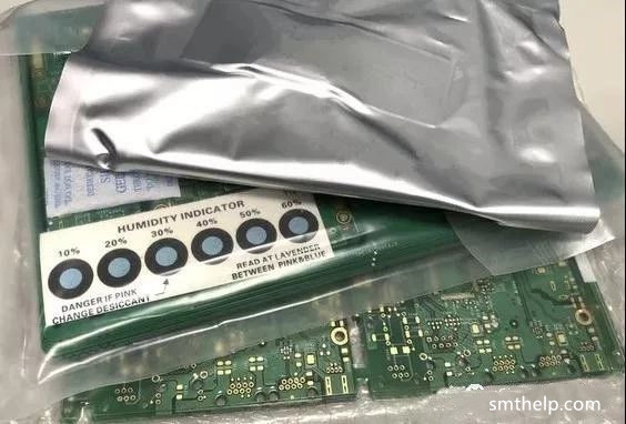
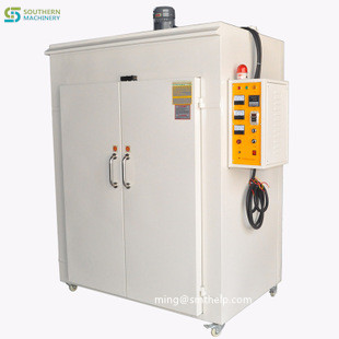
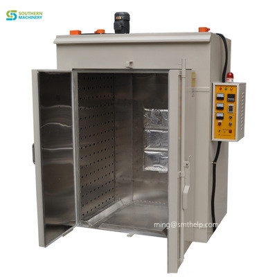
After the PCB is manufactured, it has a shelf life. If the shelf life is exceeded, the PCB needs to be baked. Otherwise, it is easy to cause the PCB to explode when the PCB is produced on the SMT.
Baking can eliminate the internal stress of the PCB, which is to stabilize the size of the PCB. The baked board has a relatively large improvement in warpage.
Advantages of baking: After baking, the moisture in the pad can be dried, the welding effect is enhanced, and the welding and repair rate are reduced.
Disadvantages of baking: The color of the PCB board may change, affecting the appearance.
The main purpose of PCB baking is to remove moisture and remove moisture from the PCB.
First, the specification of PCB management
1, PCB unpacking and storage
(1) PCB board seal can be directly used online within 2 months of unopened manufacturing date
(2) PCB board manufacturing date is within 2 months, the date of unpacking must be marked after unpacking
(3) PCB board manufacturing date is within 2 months, after opening, it must be used within 5 days.
2, PCB baking
(1) If the PCB is sealed and unsealed for more than 5 days within 2 months of the date of manufacture, please bake at 120 ± 5 °C for 1 hour.
(2) If the PCB is more than 2 months from the date of manufacture, please bake at 120 ± 5 °C for 1 hour before going online.
(3) If the PCB is more than 2 to 6 months from the date of manufacture, please bake at 120 ± 5 °C for 2 hours before going online.
(4) If the PCB is more than 6 months to 1 year before the date of manufacture, please bake at 120 ± 5 °C for 4 hours before going online.
(5) The baked PCB must be used within 5 days (input to IR REFLOW). After the bit is used, it needs to be baked for another hour before it can be used.
(6) If the PCB exceeds the manufacturing date of 1 year, please bake at 120 ± 5 °C for 4 hours before going online, and then send it to the PCB factory for re-spraying before it can be used.
3, PCB baking method
(1) Large PCB (16 PORT and above including 16 PORT), placed in a flat format, with a maximum of 30 sheets in a stack, and the oven is opened within 10 minutes after baking. The PCB is placed in a flat and natural cooling (requires pressure to prevent the bay fixture)
(2) Small and medium-sized PCB (8PORT below 8PORT) is placed flat, the maximum number of stacks is 40 pieces, the number of uprights is not limited, the oven is opened within 10 minutes after baking, and the PCB is placed flat and naturally cooled (requires pressure protection) Banwan fixtures)
PCB-baked-machine-1
Second, the preservation and baking of PCBs in different regions
The specific storage time and baking temperature of the PCB are not only related to the production capacity and manufacturing process of the PCB manufacturer, but also have a great relationship with the region.
The PCB made by the OSP process and the pure immersion gold process generally has a shelf life of 6 months after packaging, and is generally not recommended for the OSP process.
The storage and baking time of PCB has a great relationship with the area. The humidity in the south is generally heavier. Especially in Guangdong and Guangxi, there will be “returning to the south” weather every year in March and April. It is very wet at this time. The PCB must be used up within 24 hours of exposure to air, otherwise it will be easily oxidized. After normal opening, it is best to use up to 8 hours. For some PCBs that need to be baked, the baking time is longer. In the northern regions, the weather is generally dry, the PCB storage time will be longer, and the baking time can be shorter. The baking temperature is generally 120 ± 5 ° C baking, baking time is determined according to the specific circumstances.
If you need to know more about PCB drying and PCB-baked-machine machin, please contact us.
Southern Machinery (SMTHELP), which specializes in SMT machines and spare parts. SMTHELP has more than 20 years of experience in the electronics processing equipment industry. Customers all over the world, and win the trust and praise of customers. Long-term customers include BOSCH in Spain and India, DIXION in India, Panasonic in Mexico, Samsung and Cliptechin Brazil.
With the SMTHELP industry experience, philosophy and professional team, adhere to the “One-Stop Solution” belief to serve customers in the electronics processing industry, providing customers with cost-effective, high quality spare parts and equipment with stable performance from China, saving customers time And cost. truly one-stop solution services.
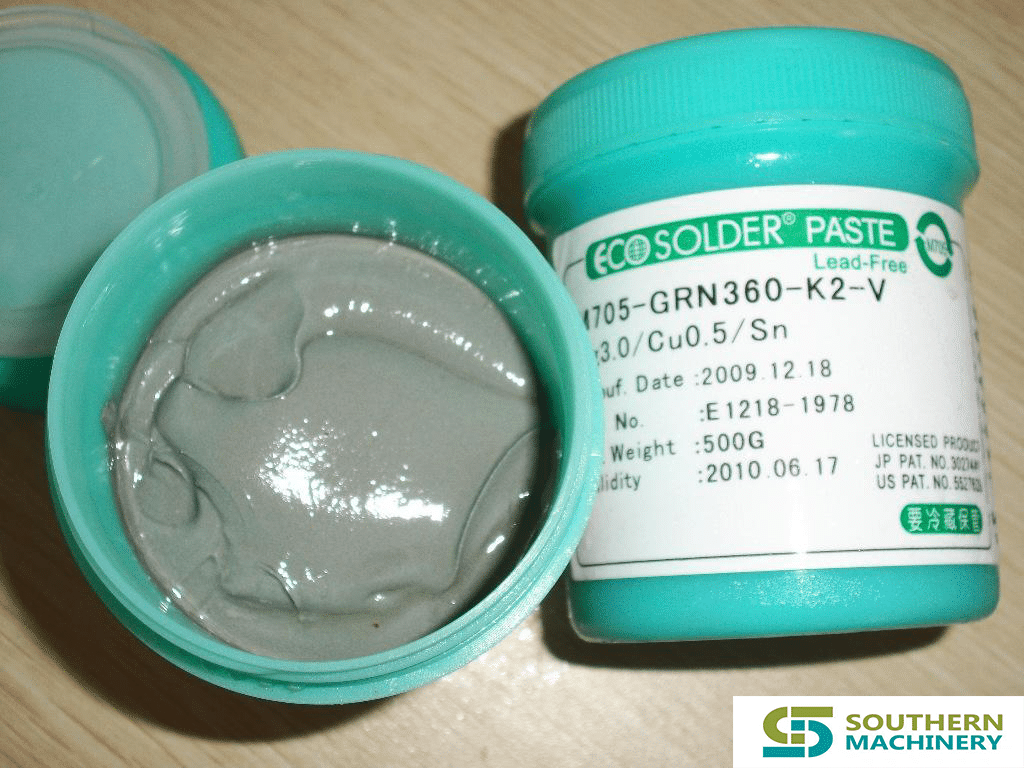
In SMT PCB production, solder paste printing is a critical step. Since the solder paste is used to directly form the soldering joint, the quality of solder paste printing affects the performance and reliability of the surface mount assembly. Quality solder paste printing guarantees a quality solder joint and final product. Statistics demonstrate that 60% to 90% of soldering defects are related to solder paste printing defects. So it is very important to understand what causes defects in solder paste printing.
ItemFactorsAnalysis1Solder PastePowder formationThe irregular shape of solder powder will easily clog stencil apertures. This will cause a big slump after printing. It can also cause solder ball and short bridge defects after reflow.
A spherical shape is best, especially for fine-pitch QFP printing.Particle SizeIf the particle size is too small, the results will be poor paste adhesion. It will have a high oxygen content and cause a solder ball after reflow.
The particle size should be controlled to about 25 ~ 45 μm in order to meet the requirements for fine-pitch QFP soldering, If the partical size desired is 25 to 30 μm, it should applied with less than 20 μm solder paste for an ultra fine-pitch IC.FluxFlux contains a thixotropic agent, which allows the solder paste to have pseudoplastic flow characteristics. Since the viscosity decreases when the paste passes through the stencil apertures, the paste can be applied to the PCB pads rapidly. When the external force stops, the viscosity will recover to ensure no deformation occurs.
The flux in the solder paste should be controlled to between 8 and 15 percent. A lower flux content will result in excess amount of solder paste applied. Conversely, a high flux content will result in an insufficient amount of solder applied.2StencilThicknessA stencil that is too thick will cause a solder bridge short.
A stencil that is too thin will cause an insufficient solder to be applied.Aperture sizeWhen the stencil aperature size is too big, a solder bridge short can occur.
When the stencil aperature size is too small, and insufficient solder paste will be applied.Aperture shapeIt is best to use a circular-shaped stencil aperture design. Its size should be slightly smaller than the PCB pad size, preventing a bridging defect during reflow.3Printing parametersBlade Angle Speed & PressureThe blade angle affects the vertical force applied on the solder paste. If the angle is too small, the solder paste will not be squeezed into the stencil apertures. The best blade angle should be set around 45 to 60 degrees.
A higher the printing speed means that less time will be spent in applying the solder paste through the stencil aperture surface. A higher printing speed will cause insufficient solder to be applied.
The speed should be controlled to around 20 ~ 40 mm/s.
When the blade pressure is too small, it will prevent the solder paste from being cleanly applied to the stencil.
When the blade pressure is too high, it will result in more paste leakage. The blade pressure is typically set at about 5N ~ 15N / 25mm.4Printing process controlPCB moistureIf the PCB moisture is too high, the water under the solder paste will quickly evaporate, causing the solder to splash and creating solder balls.
Dry the PCB if it was fabricated over 6 months ago. The recommended drying temperature is 125 degrees for 4 hours.Paste storageIf the solder paste is applied without a temperature recovery period, the water vapour in the surrounding environment will condense and penetrate the solder paste; this will cause the solder to splash.
Solder paste should be stored in a refrigerator at 0 to 5 degrees.Two to fours hours before use, place the paste in a normal temperature environment.
An article to let you know the principle of PANASONIC-MV2V(C/F/B) component recognition.
Edited by ming Gan, please contact ming@smthelp.net for more information.
principle of PANASONIC-MV2V(C-F-B) component recognition (1)principle of PANASONIC-MV2V(C-F-B) component recognition (2)principle of PANASONIC-MV2V(C-F-B) component recognition (3)principle of PANASONIC-MV2V(C-F-B) component recognition (4)principle of PANASONIC-MV2V(C-F-B) component recognition (5)
1 program composition
1) NC PROGRAM: Z-axis components are placed at X, Y positions at θ angle
2) PCB PROGRAM: substrate length, width, thickness and PIN spacing
3) ARRAY PROGRAM: Z specified components
4) PART LIBRARY: Component Information
5) MARK LIBRARY: tag information
2 NC PROGRAM
1) File name: P— [0-9, A-Z, +, -,.]
2) X, Y coordinates
3) Z No: ZA+ZB, K TYPE and Q TYPE, in single and double FEEDER at 8mm width
The difference between K TYPE and Q TYPE: * PIN, no PIN
* PITCH: K-21.5mm Q-20mm
* ORG: FULL is 1, K-Z1, Q-Z2 when HALF
FEEDER: HALF must be used when mixing single and double
Z No: Single input K TYPE: Product number, Q TYPE: Even
4) θ angle: θ1, θ2 two, θ3 origin return
Θ1:0° 90° 180° 270°
Θ2: [set angle – θ1] + correction angle Reverse time is –
5) S&R: STEP REPEAT, PATTERN REPEAT
On time is +
6) NO MOUNTING: 0-normal patch, 1-non-patch
7) SKIP BLOCK: 0 – unconditional execution, 1 to 9 – conditional jump, 7 – unconditional jump
8) MARK: 0 – no MARK, 1 – individual MARK, 2-PCB MARK, 3-PATTERN MARK
9) LAND TEACHING: 0-NO, 1-LAND TEACHING [Recommended for the second leg of each side]
10) BAD MARK: 0-NO, 1-BAD MARK [SENSOR] 2-BAD MARK [PCB CAMERA]
11) PROGRAM OFFSET: X=, Y=, move the first point of the patch to the camera center
The machine automatically finds PROGRAM OFFSET
12) Z ORG is normally 1 and Z No can be set
* NC PROGRAM sequence
S&R->BAD MARK->MARK/PROGRAM->ROGRAM OFFSET->MARK
3 ARRAY PROGRAM
1) File name: P— [0-9, A-Z, +, -,.]
2) Z No: Fixed cannot be changed
3) SHAPE CODE: shape coding [machine]
4) PARTS NAME: component name [person]
5) VACUUM OFFSET: NOZZLE↑ +, NOZZLE↓ – [-3~3mm]
6) MASTER Z No.: master, slave Z axis
4 PCB PROGRAM
1) File name: P— [0-9, A-Z, +, -,.]
2) X: PCB length
3) Y: PCB width
4) T: PCB thickness [NO USED]
5) Whether the PIN is used: 0-not used, 1-automatic adjustment
6) Hole spacing: X-10
7) Conveyor speed: 1[H]~8[L] speed, X, Y table speed when fully automatic control
5 MARK LIBRARY
1) SHAPE CODE: shape coding, —
X, Y: MARK size
PCB material: 0-copper foil, 1-solder
PATTERN: shape
TYPE: 0-shade, 1-binarization
6 PARTS LIBRARY
1) Shape coding: SHAPE CODE [—, 0-9, A-Z, +, -,.]
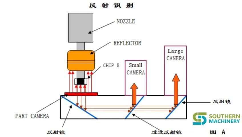
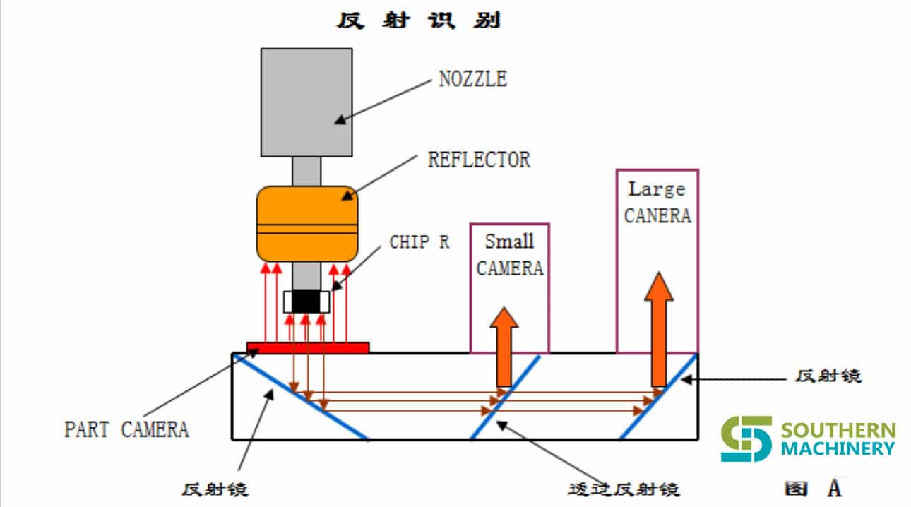
2) Component type CLASS: 1 to 99 [1 to 19 transmission recognition, 20 to 99 reflection recognition]
Reflection recognition: blue light is absorbed on the orange reflector, and the surface of the component is reflected [Figure A]
By recognizing: the white light of the halogen lamp shines on the orange reflector, and the reflector reflects the light.
Depending on the component, the edge of the component is reflected to the camera [Figure B]
* High reflection recognition accuracy, high passability through recognition, LED off when used
* For identification θ: CHIP angular deviation > 35° NG, QFP angular deviation > 25° NG
TYPE: For component color, normal condition is 1 [black best]
3) SHUTTER [Shutter]: 0-on, 1-in [Generally open]
Closed left and right to ensure component identification [Figure D]
4) Component dimensions SIZE: up, down, left, right
Hand-drawn tape to see the reverse side of the component is the same as the camera [Figure C]
5) Component thickness THICKNESS: T-component body thickness
6) Thickness tolerance TOL: T<1 is 20% T≥1 is 15%
7) HEAD SPEED: 1[H]~8[L] X, Y TABLE SPEED: 1[H]~8[L]
8) NOZZLE SELECT: 1~5
9) CAMERA: 0-S, 1-L
10) Component feed direction FEED DIRECTION: 0 to 7, 45° interval
11) Packing method: 0-PAPER [including 32mmPEELING] 1-EMBOSS 2-BULK
12) PUSHPIN: 0-NO USE 1-USE only for 8mm bandwidth
13) Number of feeds FEED COUNT: 1~4 spacing 12mm
14) Auxiliary feed: NO USE
15) Component error correction RECOVERY: 0-NO, 1-YES, 2- large parts are sucking
16) CHIP STAND: 0-NO, 1-YES
[Components stand up, thickness sensor is detected, LINE SENSOR application]
17) VACUUM OFFSET: absorbing, for components [-3mm~+3mm]
18) LEAD OUT SIZE: Up/Down Left/Right
19) LEAD PITCH: leg spacing
20) LEAD PITCH TOL: tube leg tolerance
21) LEAD COUNT: Up/Down Left/Right Legs
22) Electrode part ELECTROD: The length direction of the element is the length direction of the electrode [Fig. E]
The width direction of the component is the width direction of the electrode
23) CUT LEAD: cut tube legs SIDE: 1~4, there are cut legs on the side
COUNT: Cut off: POSTION: Position [Figure F]
1,Please visit : www.smthelp.net
2, Find us more: https://www.facebook.com/autoinsertion
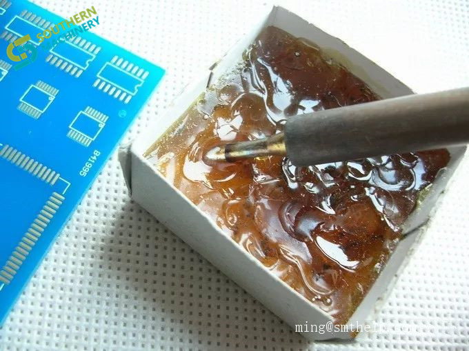
Depth analysis: What are the factors that affect the thickness of SMT press solder paste printing?
In the solder paste printing machine, sometimes the printed solder paste is very thin, which causes the product to fall off due to too little solder paste after the furnace is finished. So how is this phenomenon caused? Below I will analyze some specific reasons for everyone.
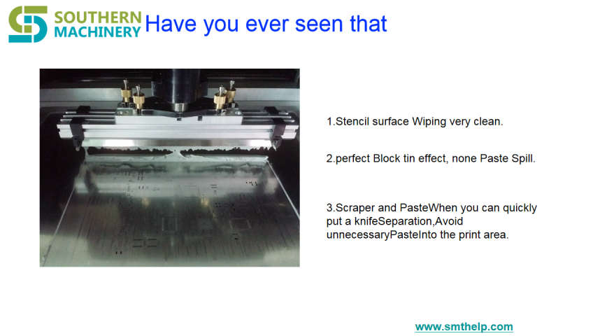
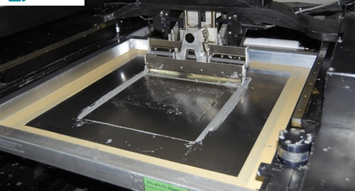
First, the quality of the steel plate — stencil printing is contact printing, so the stencil thickness and opening size determine the amount of solder paste printing, too much solder paste will produce bridging, too little solder paste will occur solder deficiency or solder joint, template The shape of the opening and the smoothness of the opening also affect the quality of the release. The template opening must have the bell mouth down, otherwise the solder paste will be taken from the chamfered corner of the bell when the mold is released. DEK accessories
solder paste printingsolder paste printing
Second, the printing process parameters — solder paste is a thixotropic fluid, with viscosity, when the scraper moves forward at a certain speed and angle, push the solder paste to roll in front of the scraper, the need to inject solder paste into the mesh or leak hole The pressure, the viscous friction of the solder paste causes the solder paste to shear at the intersection of the squeegee and the stencil, and the shear force reduces the viscosity of the solder paste, which facilitates the smooth injection of the solder paste into the mesh. There is a certain constraint between the speed of the blade, the pressure of the blade, the angle of the blade and the stencil, and the viscosity of the solder paste. Therefore, only by properly controlling these parameters can the printing quality of the solder paste be ensured.
How SMT workshop planning? It turned out to be so useful.
How SMT workshop planning!
And only after the plant began production found that some areas have not planned beforehand, need to be adjusted, resulting in a waste of human and financial resources and valuable production time.
Therefore, it is important to check in advance SMT factory layout, especially for new SMT factory business, because there is no experience in SMT plant layout, the need to pay attention to the elements is not very clear, if we find a problem in the layout after production point, will cause some unnecessary losses.
So, when doing layout SMT plant, what to pay attention to what matters in advance to do to prepare? Here actual cases where we work to and we explore this problem.
Case
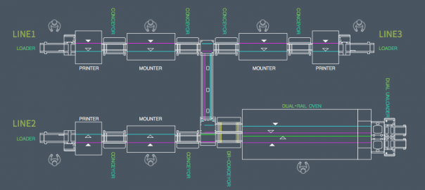
planning SMT line configure
the client recent planning new on two identical SMT production line, specific device configuration (see FIG. 1) and the size of the apparatus is as follows: According to Figure 1 can be seen, the maximum width of the production line equipment is 1.71 m, the length of all devices sum is 13.6 meters, will add future planning a production line (line bulk on equipment configuration).
Situation Workshop
Workshop length 36 m, width of 12 m, an area of 432 m2, on the ground floor of the factory. Currently common ground for the shop floor, and no established anti-static system, can not meet the requirements of SMT antistatic workshop, but two conductive ground terminals, can establish subsequent workshops antistatic SMT system. Further, there is no air conditioning workshop and humidifiers, can not meet the requirements of SMT workshop temperature and humidity control. There workshop ventilation system, back to meet the requirements of the reflow furnace equipment. Workshop sufficient power to meet the electricity needs of all equipment in the workshop. There are two entrances whole plant, as are required to meet the equipment, raw materials and semi-finished channel. Special materials warehouse in another workshop, the need for planning. Good lighting conditions in the workshop, to meet the brightness of the SMT shop lighting requirements all stations. Whole plant layout situation shown in Figure 2.
Customer requirements
1, the current new move into production lines and related aids, regional positioning;
2, the whole plant to meet future erection and production requirements three production lines, without planning zone realignment;
3, each production line starting position as consistent as possible, so that the whole plant orderly arranged in three lines.
Subject of
analysisthe customer’s request, we first analyzed how the production line positioning; and before locating the production line, we consider the following points:
1, SMT equipment should avoid column and they maintain a certain distance, the distance is equipment installed at least after a good feed material by a vehicle;
2, SMT crossing equipment required for frame division pitch, and the crossing equipment to extend outwardly after the device installed above the material 50 cm;
3, optimal spacing of the two lines spaced more than 1.2 meters between the outer frame;
4, check the wire tail is generally a repair plan area, quality control personnel can perform sampling line tail region.
Based on the above considerations, the length of each line should be at least 13.6 meters (without regard to the maintenance area and the tail, the case where the sampling area and the thread area kanban), the width should be 2.7 meters (SMT feeding both surfaces), specifically as shown in Figure 3.
Therefore, the production line is positioned in substantially considering plant shown in FIG. 4.
Some details of the requirements of SMT plant layout
after determining the approximate location of the production line, when the need to consider some details of SMT production line requirements, and then to determine the exact location and the location of other auxiliary equipment SMT line.
First, we analyzed the SMT line position and aids required for each area requirements: 1, fire extinguisher drop zone;
fire extinguishers to be placed around the side of the post and SMT plant, placed according to the requirements of fire regulations.
2, the car rack placement region; car rack replacement for SMT production line models and switching material, in order to facilitate production and to improve the efficiency of replacement materials, preferably the vehicle is placed near the rack placement machine.
3, stock units rest area;
stock table mainly used in the production process and dryer materials stock preparation before switching, therefore, to be placed near the preparation station placement machine, and the best car rack together, Preparation facilitates directly on the car frame after a good feed material.
4, the shelf rest area printing station;
printing station for positioning the shelf aids in the production of printing presses, such as wipes, paste, alcohol, etc., to be placed in the vicinity of the printing press to facilitate removal use, improve Productivity.
region comprising placing solder paste storage refrigerator, solder paste mixer, paste warmed cabinets, can be placed next to the plant as required or uprights placed around a fixed area of the plant, However, to facilitate the operator to take place.
6, visual inspection after the furnace area, maintenance area;
in order to facilitate visual inspection after reflow and rework semifinished product, a shelf generally placed in the furnace, designed for the visual inspection of the furnace and rework.
7, screen placement area;
drop zone comprises a mesh screen plate was placed cabinet, stencil cleaningmachine, inspection tools, screen, stencil for storing, cleaning and inspection screen tension, etc., while in the region as much as possible to facilitate the production screen to take place.
8, garbage drop zone;
Production waste mainly from two parts, wipes and the like used in one printing operation, the second is to replace the waste tray and waste material produced with the like. Garbage two parts is generated to be placed separately, specialized recycling, in particular waste presses used. Thus, waste area may be placed next to the press machine or patch, or set beside the column region refuse placed separately placed.
9, kanban placement region;
kanban including the SMT billboards and other signage quality management, may be centrally located on the entrance into the shop, and also set up the production line Kanban state in which each head of the line, in order to view the producers and managers, promptly understand the current state of production status and quality SMT workshop and so on.
10, product placement area;
include products produced finished products in two parts, to separate the two partial regions divided out, strictly distinguished, in order to avoid confusion.
11, SMT placement of spare areas;
Nozzle including the SMT spare parts, a motor, a belt, cylinder or the like, to be placed in a special area, to facilitate the production of access.
12, location area temperature and humidity;
temperature and humidity conditions in order to better understand the SMT plant, depending on the size of the workshop area, several appropriately set the temperature and humidity measurement area, generally placed on the production line next to the column or wall.
13, SMT workshop office area;
let engineers and technicians and management personnel in office SMT shop floor, which can solve the problem on technology and management encountered in the production, to ensure the smooth operation of the SMT production lines.
14, anti-static protection area;
entry into SMT workshop area must have good anti-static measures. You may delineate the area in front of the plant, including the replacement of static clothing, shoes, hats and so on each employee’s locker. Also, the establishment of regional designed to test the static ring in SMT workshop at the entrance, so that each employee to do static loop testing and record test results before going to work. Based on the above analysis, the results of this SMT plant layout is shown in Figure 5.
In addition, SMT workshop also meet other requirements: 1, anti-static processing;
shop floor must be anti-static treatment, a common anti-static conductive flooring and paint and other ordinary places, customers can choose according to the actual situation. In addition, anti-static system must be set up in the workshop, to meet the requirements of the entire anti-static SMT workshop.
2, air-conditioning and a humidifier; SMT workshop to meet the requirements of temperature and humidity control.
3, the material management requirements;
in the warehouse, with particular attention to the way the material is stored, reel packaging methods, the use of hook-type place, wetting elements employed Cabinets for placement shelves to be treated with anti-static manner.
4, patch equipment gas and electrical circuitry;
preferably introduced directly from the production line at the down side of the roof, is arranged below the gas passage in the device and circuit wrapped with wire groove.
5, the ventilation system requirements;
needs to be installed to meet the requirements of the three power lines of the blower, and the third exhaust port reserved line.
Results
1, according to the size of production line and the size of the entire plant SMT, completed the reasonable position of the production line; and
2, for aids, regions, etc. SMT production lines need to make the corresponding position location; 3, according to the SMT the characteristics of the plant, some of the necessary factors to consider in planning, in particular, anti-static; 4, in accordance with the requirements of the current situation and future development of the factory has been take into consideration, unified planning.
Summary
For SMT plant layout, but also requires a combination of size and product requirements and other plants to consider a number of factors, but to stimulate here.