Circuit board, PCBA cleaning, is it really important for EMS (Electronic Manufacturing Service)?
Edited by Ming: ming@smthelp.net
“Cleaning” is often overlooked during board (PCB) PCBA manufacturing and is considered to be not a critical step. However, with the long-term use of the product on the client side, the problems caused by the ineffective cleaning in the early stage caused many failures, and the rework or recall of the product caused a sharp increase in operating costs. Below, SMTHELP briefly explains the role of PCBA cleaning of circuit boards (circuit boards).
PC BA (Printed Circuit Assembly) has a number of process stages in the production process, each stage is contaminated to varying degrees, so the surface of the PCBA of the circuit board (circuit board) is left with various deposits or impurities, which will lower the product. Performance, and even cause product failure. For example, in the process of soldering electronic components, solder paste, flux, etc. are used for auxiliary soldering, and residues are generated after soldering, and the residue contains organic acids and ions, etc., in which organic acids corrode the circuit board (circuit board) PCBA, and The presence of electrical ions can cause short circuits and cause product failure.
There are many kinds of contaminants on PCB (PCB) PCBA, which can be classified into two types: ionic and non-ionic. The ionic pollutants are exposed to moisture in the environment, and electrochemical migration occurs after energization, forming a dendritic structure, resulting in a low resistance path and destroying the PCBA function of the circuit board (circuit board). Non-ionic contaminants can penetrate the insulating layer of PC B and grow dendrites under the surface of the PCB. In addition to ionic and non-ionic contaminants, there are also particulate contaminants such as solder balls, floating spots in solder baths, dust, dust, etc. These contaminants can lead to reduced solder joint quality, sharp solder joints during soldering, and Porosity, short circuit and many other undesirable phenomena.
With so many pollutants, which ones are the most concerned? Fluxes or solder pastes are commonly used in reflow and wave soldering processes. They are mainly composed of solvents, wetting agents, resins, corrosion inhibitors and activators. Thermally modified products must be present after soldering. In all the pollutants, the post-weld residue is the most important factor affecting the quality of the product. The ionic residue tends to cause electromigration to reduce the insulation resistance, and the rosin resin residue is easy to adsorb. Dust or impurities cause an increase in contact resistance, and in severe cases, open circuit failure, so strict cleaning must be performed after welding to ensure the quality of PCBA of the circuit board (circuit board).
In summary, the cleaning of the circuit board (PCB) PCBA is very important, and “cleaning” is an important process that is directly related to the quality of the PCB (circuit board) PCBA, which is indispensable.
After the circuit board is cleaned, the board surface turns white, what should we do?
Edited by Ming: ming@smthelp.net
First, the board surface is whitish after cleaning:
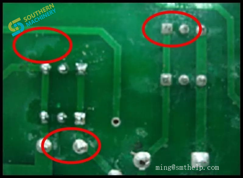
In the electronic component manufacturing process, the PCBA circuit board is often over-wave soldered, and after the manual cleaning agent is used for cleaning, the board surface appears white (Figure 1).
After the cleaning of the PCBA solder joints, the white surface of the board surface appears after being placed, and the white mark is scattered around the solder joints, which seriously affects the appearance acceptance.
Second, the reason for the whitish surface of the board after cleaning:
White residue is a common contaminant on PCBA and is generally a by-product of flux. Common white residues are polymerized rosin, unreacted activator, and lead metal chloride or bromide, which react with flux and solder. These substances expand in volume after moisture absorption, and some substances also hydrate with water. White residue is becoming more and more obvious. It is extremely difficult to remove these residues on the PCB. If the temperature is too hot or high, the problem is more serious. The infrared spectroscopy analysis of the rosin and residue on the PCB surface before and after the soldering process confirms the process. .
Regardless of whether the board has white residue after cleaning, or if the white material appears after the no-clean circuit board is stored, or the white substance on the solder joint found during the repair, there are four cases:
Rosin in the flux: Most of the white matter produced after the cleaning is not clean, stored, and the solder joint fails, is the inherent rosin in the flux. Rosin is usually a transparent, hard and brittle solid material with no fixed shape, not a crystal. Rosin is thermodynamically unstable and has a tendency to crystallize. After the rosin crystallizes, the colorless transparent body becomes a white powder. If the cleaning is not clean, the white residue may be a crystalline powder formed by the rosin after the solvent is volatilized.
When the PCB is stored under high humidity conditions, when the absorbed moisture reaches a certain level, the rosin gradually changes from a colorless and transparent glass state to a crystalline state, and a white powder is formed from a viewing angle.
The essence is still rosin, but the shape is different, still has good insulation, and will not affect the performance of the board. The abietic acid and halide (if used) in the rosin are used together as an active agent. Synthetic resins generally do not react with metal oxides below 100 ° C, but react rapidly when the temperature is higher than 100 ° C. They volatilize and decompose faster, and have low solubility in water.
Rosin denature: This is the substance produced by the reaction of rosin and flux during the welding process, and the solubility of this material is generally poor, it is not easy to be cleaned, and it stays on the board to form a white residue. But these white substances are all organic, still guarantee the reliability of the board.
Organometallic salt: The principle of removing the oxide of the welding surface is that the organic acid reacts with the metal oxide to form a metal salt soluble in liquid rosin. After cooling, it forms a solid solution with the rosin, and is removed together with the rosin in the cleaning.
If the welding surface and parts are highly oxidized, the concentration of the product after welding will be high. When the degree of oxidation of the rosin is too high, it may remain on the board together with the undissolved rosin oxide. At this time, the reliability of the board will be reduced.
Metallic inorganic salts: These may be metal oxides in solders and halogen-containing active agents in flux or solder paste, halide ions in PCB pads, halide ion residues in the surface coating of components, halogen-containing materials in FR4 materials. The substance formed by the reaction of the halide ion released at a high temperature generally has a small solubility in an organic solvent.
In the assembly process, it is highly probable that the halogen-containing flux is used for the electronic auxiliary materials (although the supplier provides environmentally friendly flux, but the halogen-free flux is still relatively small), and the surface of the board remains after welding. Halogen-based ions (F, Cl, Br, l). These ionic halogen residues, which are not themselves white, are not sufficient to cause whitening of the surface. These substances form strong acids when exposed to water or moisture. These strong acids begin to react with the oxide layer on the surface of the solder joints to form acid salts, which are white substances that are seen.
Third, after the circuit board is cleaned, the board surface is whitened:
1, the general solution:
Washing method Note: When washing the PCB, the PCBA should be tilted. Do not lay it flat. You can place the paper in the washing station, so that most of the washed solution will flow down;
Do not wash the plate repeatedly for repeated times, and increase the frequency of replacement depending on the situation;
3, and then start from the washing water formula, you can ask the supplier to improve the formula, improve the cleaning degree and dissolution volatility.
How to completely solve the problem of whitening of the board after cleaning the circuit board?
For the whitening problem of PCBA circuit board cleaning, water-based cleaning agent can be used to meet the corresponding cleaning equipment to deal with it. It is safe and environmentally friendly, meets the requirements of current ROHS, CE, and other environmental protection regulations. It has high cleaning efficiency and completely solves the problem of whitening.
SMTHELP :SMT Professional Manufacturer PCB Cleaning Machine
The product is suitable for use in automotive electronics, smart home products, communications electronics, consumer electronic product manufacturing process, to improve product reliability and to remove foreign bodies and electrostatic PCB surface
PCB cleaner,nozzle cleaning machine,PCB Stencil cleaning machine, Printer Cleaning Machine,pneumatic Stencil cleaning machine,fully pneumatic washing machine Manufacturer
Main content of lean factory design
The traditional way of plant layout begins with equipment and tooling, and finally considers the flow of processes. Unlike traditional factory layouts, lean factory design layout begins with the customer and then designs the process flow around the workforce.
Lean factory design should comprehensively apply the knowledge of lean production ideas, system engineering, enterprise management, etc., and use parallel technology, information technology and other means to determine the factory design plan that meets the requirements of lean production concept. The main design contents are as follows:
(1) Production line layout based on lean thinking
The design of the best production line must be independent of the current legacy workflow and should reduce or eliminate large amounts of moving time for products and materials. According to the assembly requirements, placing the part loading process on the assembly point where the material of the production line is consumed will reduce the movement and waiting time.
(2) Lean logistics system design
According to the lean production point of view, logistics is not a value-added link. Therefore, the goal of lean logistics system design is to minimize the logistics and strive to minimize the waste in the logistics process while meeting the production requirements. To break the limitations of the profession, try to set up and no intermediate inventory area, and completely follow the process flow layout. All ideas that minimize the amount of movement and optimize the flow of the product should be tested. Ultimately, a practical and appropriate approach should be taken to finalize the production line in order to maximize the benefits of the production process. .
(3) Lean selection and arrangement of equipment
It is necessary to fully consider the relationship between the various production links, and on the basis of realizing the capacity requirements, try to achieve a balanced production capacity and reflect the idea of lean flow. At the same time, the choice of equipment is not based on the most advanced standards, but the small size, low investment, flexibility and other indicators are put in the first place, in order to meet the needs of flexible production in the future.
(4) Lean staffing
Traditional factories use the “scheduled system” staffing, but this method increases the cost of the enterprise and reduces the response speed of the enterprise under the multi-variety and small-batch production methods. Lean factory design, it is recommended to use the least staff to achieve the same production needs, through the training of employees, so that it has a variety of skills, so that with the change in production, flexible arrangements for operators.
(5) Lean selection of auxiliary equipment
Although the fixtures and tools required for production assistance are not resource equipment, they must be considered for lean production. It must be designed to accommodate the movement of the required materials, such as the passage of the automatic loading and unloading trucks and large material containers. It is necessary to design the station to be more compact, but at the same time, the operator should be considered to be as ergonomic as possible.
In addition, the design of the lean factory should also include the planning of the public facilities of the factory, the design of the information system, etc., and should be carried out according to the specific needs of the factory and the actual situation of the enterprise.
The goal of lean plant design is to minimize waste and overload in the work process while enhancing visual communication on site.
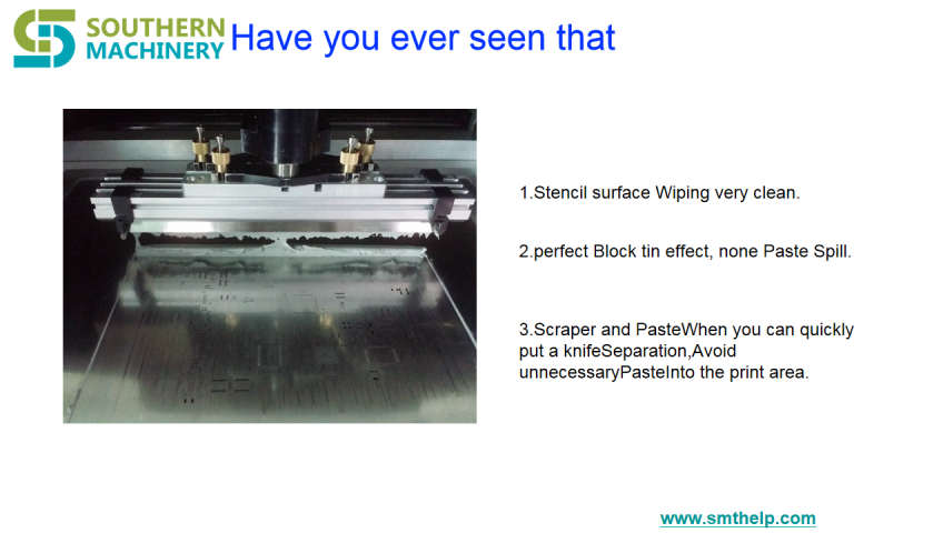
In SMT PCB production, solder paste printing is a critical step. Since the solder paste is used to directly form the soldering joint, the quality of solder paste printing affects the performance and reliability of the surface mount assembly. Quality solder paste printing guarantees a quality solder joint and final product. Statistics demonstrate that 60% to 90% of soldering defects are related to solder paste printing defects. So it is very important to understand what causes defects in solder paste printing.
ItemFactorsAnalysis1Solder PastePowder formationThe irregular shape of solder powder will easily clog stencil apertures. This will cause a big slump after printing. It can also cause solder ball and short bridge defects after reflow.
A spherical shape is best, especially for fine-pitch QFP printing.Particle SizeIf the particle size is too small, the results will be poor paste adhesion. It will have a high oxygen content and cause a solder ball after reflow.
The particle size should be controlled to about 25 ~ 45 μm in order to meet the requirements for fine-pitch QFP soldering, If the partical size desired is 25 to 30 μm, it should applied with less than 20 μm solder paste for an ultra fine-pitch IC.FluxFlux contains a thixotropic agent, which allows the solder paste to have pseudoplastic flow characteristics. Since the viscosity decreases when the paste passes through the stencil apertures, the paste can be applied to the PCB pads rapidly. When the external force stops, the viscosity will recover to ensure no deformation occurs.
The flux in the solder paste should be controlled to between 8 and 15 percent. A lower flux content will result in excess amount of solder paste applied. Conversely, a high flux content will result in an insufficient amount of solder applied.2StencilThicknessA stencil that is too thick will cause a solder bridge short.
A stencil that is too thin will cause an insufficient solder to be applied.Aperture sizeWhen the stencil aperature size is too big, a solder bridge short can occur.
When the stencil aperature size is too small, and insufficient solder paste will be applied.Aperture shapeIt is best to use a circular-shaped stencil aperture design. Its size should be slightly smaller than the PCB pad size, preventing a bridging defect during reflow.3Printing parametersBlade Angle Speed & PressureThe blade angle affects the vertical force applied on the solder paste. If the angle is too small, the solder paste will not be squeezed into the stencil apertures. The best blade angle should be set around 45 to 60 degrees.
A higher the printing speed means that less time will be spent in applying the solder paste through the stencil aperture surface. A higher printing speed will cause insufficient solder to be applied.
The speed should be controlled to around 20 ~ 40 mm/s.
When the blade pressure is too small, it will prevent the solder paste from being cleanly applied to the stencil.
When the blade pressure is too high, it will result in more paste leakage. The blade pressure is typically set at about 5N ~ 15N / 25mm.4Printing process controlPCB moistureIf the PCB moisture is too high, the water under the solder paste will quickly evaporate, causing the solder to splash and creating solder balls.
Dry the PCB if it was fabricated over 6 months ago. The recommended drying temperature is 125 degrees for 4 hours.Paste storageIf the solder paste is applied without a temperature recovery period, the water vapour in the surrounding environment will condense and penetrate the solder paste; this will cause the solder to splash.
Solder paste should be stored in a refrigerator at 0 to 5 degrees.Two to fours hours before use, place the paste in a normal temperature environment.
An article to let you know the principle of PANASONIC-MV2V(C/F/B) component recognition.
Edited by ming Gan, please contact ming@smthelp.net for more information.
principle of PANASONIC-MV2V(C-F-B) component recognition (1)principle of PANASONIC-MV2V(C-F-B) component recognition (2)principle of PANASONIC-MV2V(C-F-B) component recognition (3)principle of PANASONIC-MV2V(C-F-B) component recognition (4)principle of PANASONIC-MV2V(C-F-B) component recognition (5)
1 program composition
1) NC PROGRAM: Z-axis components are placed at X, Y positions at θ angle
2) PCB PROGRAM: substrate length, width, thickness and PIN spacing
3) ARRAY PROGRAM: Z specified components
4) PART LIBRARY: Component Information
5) MARK LIBRARY: tag information
2 NC PROGRAM
1) File name: P— [0-9, A-Z, +, -,.]
2) X, Y coordinates
3) Z No: ZA+ZB, K TYPE and Q TYPE, in single and double FEEDER at 8mm width
The difference between K TYPE and Q TYPE: * PIN, no PIN
* PITCH: K-21.5mm Q-20mm
* ORG: FULL is 1, K-Z1, Q-Z2 when HALF
FEEDER: HALF must be used when mixing single and double
Z No: Single input K TYPE: Product number, Q TYPE: Even
4) θ angle: θ1, θ2 two, θ3 origin return
Θ1:0° 90° 180° 270°
Θ2: [set angle – θ1] + correction angle Reverse time is –
5) S&R: STEP REPEAT, PATTERN REPEAT
On time is +
6) NO MOUNTING: 0-normal patch, 1-non-patch
7) SKIP BLOCK: 0 – unconditional execution, 1 to 9 – conditional jump, 7 – unconditional jump
8) MARK: 0 – no MARK, 1 – individual MARK, 2-PCB MARK, 3-PATTERN MARK
9) LAND TEACHING: 0-NO, 1-LAND TEACHING [Recommended for the second leg of each side]
10) BAD MARK: 0-NO, 1-BAD MARK [SENSOR] 2-BAD MARK [PCB CAMERA]
11) PROGRAM OFFSET: X=, Y=, move the first point of the patch to the camera center
The machine automatically finds PROGRAM OFFSET
12) Z ORG is normally 1 and Z No can be set
* NC PROGRAM sequence
S&R->BAD MARK->MARK/PROGRAM->ROGRAM OFFSET->MARK
3 ARRAY PROGRAM
1) File name: P— [0-9, A-Z, +, -,.]
2) Z No: Fixed cannot be changed
3) SHAPE CODE: shape coding [machine]
4) PARTS NAME: component name [person]
5) VACUUM OFFSET: NOZZLE↑ +, NOZZLE↓ – [-3~3mm]
6) MASTER Z No.: master, slave Z axis
4 PCB PROGRAM
1) File name: P— [0-9, A-Z, +, -,.]
2) X: PCB length
3) Y: PCB width
4) T: PCB thickness [NO USED]
5) Whether the PIN is used: 0-not used, 1-automatic adjustment
6) Hole spacing: X-10
7) Conveyor speed: 1[H]~8[L] speed, X, Y table speed when fully automatic control
5 MARK LIBRARY
1) SHAPE CODE: shape coding, —
X, Y: MARK size
PCB material: 0-copper foil, 1-solder
PATTERN: shape
TYPE: 0-shade, 1-binarization
6 PARTS LIBRARY
1) Shape coding: SHAPE CODE [—, 0-9, A-Z, +, -,.]
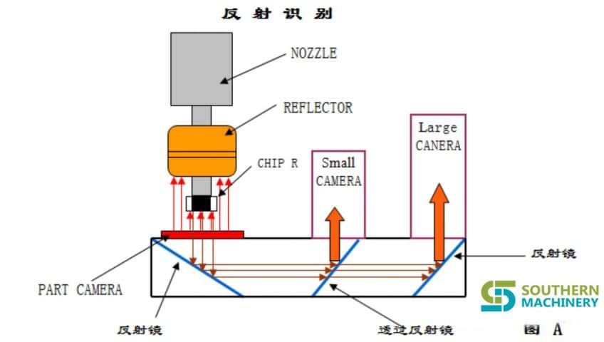
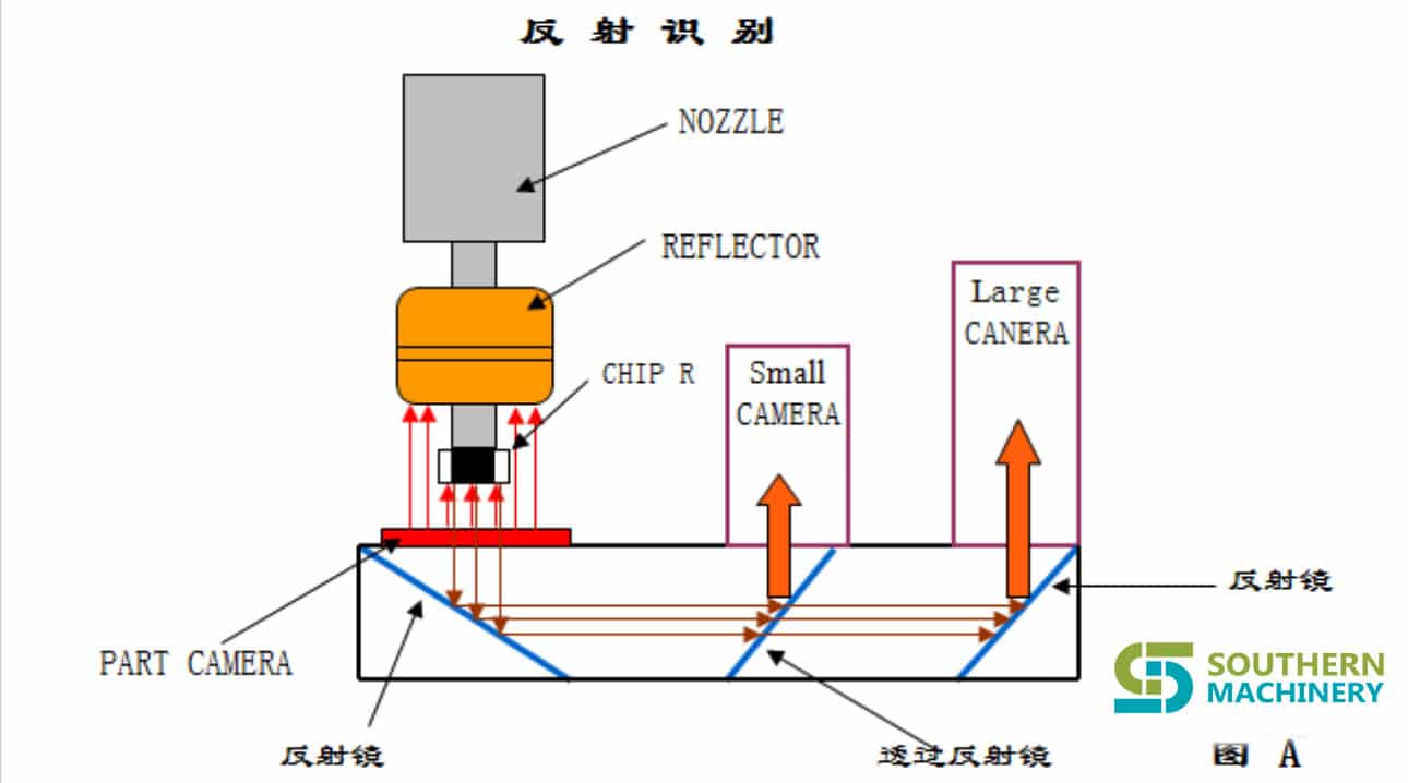
2) Component type CLASS: 1 to 99 [1 to 19 transmission recognition, 20 to 99 reflection recognition]
Reflection recognition: blue light is absorbed on the orange reflector, and the surface of the component is reflected [Figure A]
By recognizing: the white light of the halogen lamp shines on the orange reflector, and the reflector reflects the light.
Depending on the component, the edge of the component is reflected to the camera [Figure B]
* High reflection recognition accuracy, high passability through recognition, LED off when used
* For identification θ: CHIP angular deviation > 35° NG, QFP angular deviation > 25° NG
TYPE: For component color, normal condition is 1 [black best]
3) SHUTTER [Shutter]: 0-on, 1-in [Generally open]
Closed left and right to ensure component identification [Figure D]
4) Component dimensions SIZE: up, down, left, right
Hand-drawn tape to see the reverse side of the component is the same as the camera [Figure C]
5) Component thickness THICKNESS: T-component body thickness
6) Thickness tolerance TOL: T<1 is 20% T≥1 is 15%
7) HEAD SPEED: 1[H]~8[L] X, Y TABLE SPEED: 1[H]~8[L]
8) NOZZLE SELECT: 1~5
9) CAMERA: 0-S, 1-L
10) Component feed direction FEED DIRECTION: 0 to 7, 45° interval
11) Packing method: 0-PAPER [including 32mmPEELING] 1-EMBOSS 2-BULK
12) PUSHPIN: 0-NO USE 1-USE only for 8mm bandwidth
13) Number of feeds FEED COUNT: 1~4 spacing 12mm
14) Auxiliary feed: NO USE
15) Component error correction RECOVERY: 0-NO, 1-YES, 2- large parts are sucking
16) CHIP STAND: 0-NO, 1-YES
[Components stand up, thickness sensor is detected, LINE SENSOR application]
17) VACUUM OFFSET: absorbing, for components [-3mm~+3mm]
18) LEAD OUT SIZE: Up/Down Left/Right
19) LEAD PITCH: leg spacing
20) LEAD PITCH TOL: tube leg tolerance
21) LEAD COUNT: Up/Down Left/Right Legs
22) Electrode part ELECTROD: The length direction of the element is the length direction of the electrode [Fig. E]
The width direction of the component is the width direction of the electrode
23) CUT LEAD: cut tube legs SIDE: 1~4, there are cut legs on the side
COUNT: Cut off: POSTION: Position [Figure F]
1,Please visit : www.smthelp.net
2, Find us more: https://www.facebook.com/autoinsertion
Automated optical inspection machine (AOI) is a new type of testing technology. It has
developed very rapidly in recent years. The structure of AOI consists of four parts: workbench, CCD camera system, electromechanical control and system software. When testing, firstly, the circuit board to be tested is placed on the workbench of the AOI machine, and the detection
procedure of the product to be detected is called out through positioning. The X/Y workbench
will send the circuit board under the lens according to the command of the setting program. With the help of the special light source, the lens will capture the image required by the AOI system and analyze it, then the processor will move the lens toward the lens. The next position is
collected for the next image and then analyzed, and the image is subjected to continuous
analysis and processing to obtain a higher detection speed. The process of AOI image
processing essentially digitizes the extracted image, and then compares it with the pre-stored “standard”. After analysis and judgment, it finds the defect to make a position prompt, and at the same time generates image text, and the operator further confirms or sends the repair station. Overhaul
How to remove the misprinted solder paste on the PCB surface?
Prepared by Ming
ming@smthelp.net This article describes that paying attention to some details can often prevent common problems in assembly processes and equipment selection.
Question: Can I use a small spatula to remove misprinted solder paste from the board? Will this get the solder paste and small tin beads into the holes and small gaps?
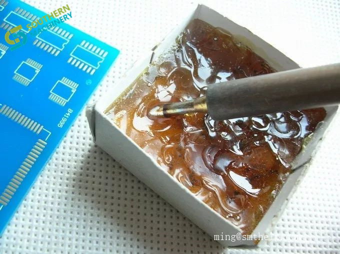
Answer: Using a small spatula to remove the solder paste from the misprinted board may cause some problems. It is generally practicable to immerse the misprinted board in a compatible solvent, such as water with an additive, and then remove the small tin beads from the board with a soft brush. I prefer to soak and wash repeatedly instead of violent dry brush or shovel. After the solder paste is printed, the longer the operator waits to clean the misprint, the harder it is to remove the solder paste. Misprinted boards should be placed in the soaking solvent immediately after the problem is discovered, as the solder paste is easily removed before it is dried.
Avoid wiping with a strip of cloth to prevent solder paste and other contaminants from smearing on the surface of the board. After soaking, brushing with a gentle spray can often help remove unwanted tins. It is also recommended to dry with hot air. If a horizontal stencil cleaner is used, the side to be cleaned should face down to allow the solder paste to fall off the board.
As usual, note that some details can eliminate undesirable conditions, such as misprinting of the solder paste and removal of the solder paste from the board. It is our goal to deposit the right amount of solder paste at the desired location. Stained tools, dry solder paste, and misalignment of the stencils and plates can cause undesirable solder paste on the underside of the stencil or even the assembly. During the printing process, the template is wiped with a certain pattern between printing cycles. Ensure that the template is seated on the pad, not on the solder mask, to ensure a clean solder paste printing process. On-line, real-time solder paste inspection and inspection prior to reflow after component placement are process steps that reduce process defects prior to soldering.
For fine-pitch stencils, if damage is caused between pins due to thin stencil cross-section bending, it can cause solder paste to deposit between the pins, causing printing defects and/or short circuits. Low viscosity solder paste can also cause printing defects. For example, high operating temperatures or high blade speeds can reduce the stickiness of the solder paste during use, resulting in printing defects and bridging due to excessive solder paste deposition.
In general, the lack of adequate control of materials, solder paste deposition methods and equipment are the main causes of defects in the reflow soldering process.
Question: What type of assembly board depaneling equipment provides the best results?
Answer: There are several sub-board systems that offer a variety of techniques for slab assembly boards. As a rule, there are many factors that should be considered when selecting such a device. Regardless of whether there is routing, sawing or blanking to separate individual panels from the composite panel, stable support during the splitting process is the most important factor. Without support, the resulting stress can damage the substrate and solder joints. Distorting the plate, or stressing the assembly during the splitting, can result in hidden or significant defects. While sawing often provides minimal clearance, shearing or die cutting with tools can provide cleaner, more controlled results.
In order to avoid component damage, many assemblers attempt to maintain component solder joints at least 5.08 mm from the edge of the board when the splitter is required. Sensitive ceramic capacitors or diodes may require extra care and consideration.
1,Please visit : www.smthelp.net
2, Find us more: https://www.facebook.com/autoinsertion
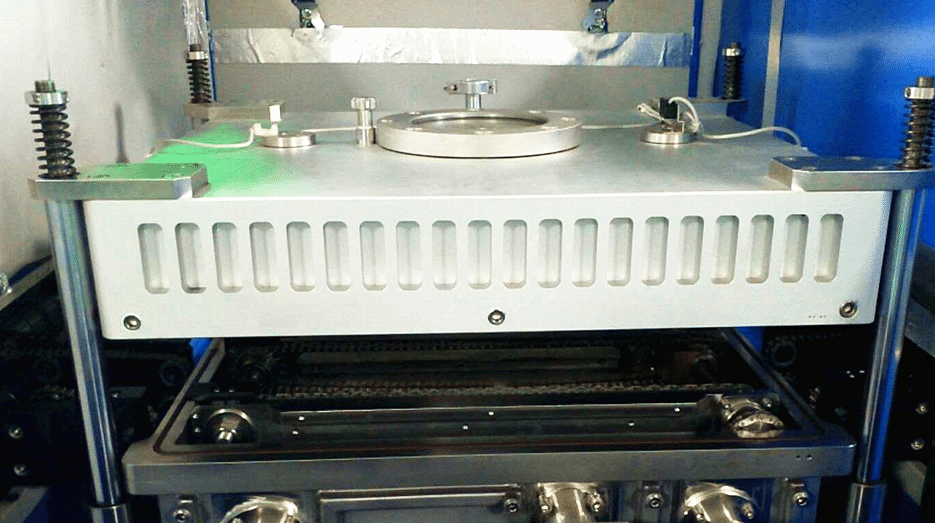
Applications: IGBT packaging, LED eutectic, solder paste process, high clean soldering process, laser diode package, hybrid integrated circuit package, package cover package, MEMS and vacuum package.
Industry application: S-V series vacuum reflow soldering machine is an ideal choice for R&D, process research and development, high-capacity production, and is the best choice for high-end R&D and production in military enterprises, research institutes, universities, aerospace and other fields.The product weld void rate is as low as 3% or less.
Features:
It adopts imported heating parts, uniform temperature and high thermal compensation efficiency. It is suitable for CSP, BGA, automobile lamp, UV lamp, LED flip chip process, laser device package, IGBT power device package process soldering;
Special wind wheel design, large air exchange and stable wind speed;
Each temperature zone adopts forced independent circulation, independent PID control, and independent heating mode to make the furnace cavity temperature accurate and uniform, and the heat capacity is large: 4, the temperature rises quickly, from room temperature to working temperature ≦ 30 minutes;
Imported high-quality high-temperature high-speed motor has stable wind, low vibration and low noise;
The furnace body adopts double cylinder (electric push rod) jacking device, which is safe and reliable; 7, chain, mesh belt synchronous constant speed transportation, using frequency conversion precision high speed; 8, special high-quality aluminum alloy rail design, small deformation, chain automatic refueling device; 9, UPS power-off protection function, to ensure the normal output of the PCB after power-off, not damaged;
Powerful software function, monitor and measure the temperature of the PCB board online, and analyze, store and print the data curve at any time;
11, industrial control PC and PLC communication using MODBUS protocol, work stable, to prevent the phenomenon of crash;
12, automatic monitoring, display equipment working status, you can make correction parameters at any time;
Special patented furnace design, good thermal insulation, and the lowest power consumption in the same industry;
The patented guide rail is not deformed at high temperature, and the three-wire rod synchronously widens the structure, effectively ensuring that the guide rails are parallel, preventing the board from falling, the occurrence of the card board, no cleaning, and easy adjustment. The adjustment operation can be performed both automatically and manually.
Standard chain and net chain synchronous iso-speed parallel transportation, can process single-sided and double-sided PCB boards, and optional double-rail transportation system.
The automatic width adjustment system adopts closed-loop PID control, which can be automatically adjusted to the required width according to the parameters input by the computer, and the accuracy can reach 0.2mm.
Due to the modular design of each temperature zone, hot air motor and heating wire are convenient for maintenance and repair.
18, strong cooling air cooling, cold air exchange fast, uniform wind speed, slope can be controlled by frequency conversion, tin point is smooth and bright;
The nitrogen flow meter can monitor the nitrogen flow at any time;
20, in the traditional SMT welding process, to improve, reduce the voids in the solder, the void rate can reach less than 5%;
21, high-quality products for mass production, the shortest product welding process cycle is 30S, to maintain continuous production;
At the same time, the equipment meets the traditional SMT process production configuration, nitrogen welding process and air welding process;
The vacuum part is independently controlled, and can be configured according to the process of the product, or can be shielded with the traditional process product to close this function;
Model
S-V8000
Heating part parameters
Number of pre-zones
8/8
Heating zone length
3000mm
number of cooling zones
2/2
Vacuum zone
Number of vacuum zones
1
Product size
smallest size:100*100MM;biggest size:300*350MM,
vacuum
10-100pa
Vacuum pumping speed
40m³/h Adjustable
Visual observation window
1
Heating system (optional)
Space maximum temperature 350 degrees
Flux recovery system
Reduces equipment maintenance and increases component life
System Control
Touch Screen + Siemens PLC
Process control action
Vacuuming time, vacuum pressure, vacuum pumping speed, vacuum maintenance time, deflation time free control setting
Transmission part parameters
Mesh belt width
500MM
Transport rail adjustment range
50-450MM
Transmission direction
L-R(R-L)
Transportation height
900±20MM
Transmission mode
mesh belt + chain transmission
Transmission speed
300-2000mm/min
power supply
Three five-line 380V 50/60HZ
Starting power
52KW
Normal work consumption Approx
Approx.10KW
Heating time
20min
Temperature control range
Room temperature -350 degrees
Temperature control
Full computer PID closed loop control, SSR drive
Machine control mode
PC+PLC
Temperature control accuracy
±1
PCB board temperature distribution difference
±1-2
Cooling method
Cold water cooling
Alarm temperature
Abnormal temperature (super high temperature or ultra low temperature after constant temperature)
Tricolor light indication
Three-color signal indicator: yellow – warming green – constant temperature red – abnormal
Electronics are an integral part of our daily lives. Everything from our smart phones to our cars includes electronic components. At the heart of these electronics is the printed circuit board, also known as a PCB.
Most people recognize printed circuit boards when they see them. These are the small green chips covered in lines and copper parts you’ll find at the heart of gutted electronic devices. Made with fiberglass, copper lines and other metal parts, these boards are held together with epoxy and insulated with a solder mask. This solder mask is where that characteristic green color comes from.
However, have you ever observed those boards with components solidly stuck on? Never regard them as just decorations of a PCB board. An advanced circuit board won’t be able to give its functionality until components are mounted on it. A PCB with components mounted on is called an assembled PCB and the manufacturing process is called PCB assembly or PCBA for short. The copper lines on bare board, called traces, electrically link connectors and components to each other. They run signals between these features, allowing the circuit board to function in a specifically designed way. These functions range from the simple to the complex, and yet the size of PCBs can be smaller than a thumbnail.
So how exactly are these devices made? The PCB assembly process is a simple one, consisting of several automated and manual steps. With each step of the process, a board manufacturer has both manual and automated options from which to choose. To help you better understand the PCBA process from start to finish, we’ve explained each step in detail below.
The first step of PCB assembly is applying a solder paste to the board. This process is like screen-printing a shirt, except instead of a mask, a thin, stainless-steel stencil is placed over the PCB. This allows assemblers to apply solder paste only to certain parts of the would-be PCB. These parts are where components will sit in the finished PCB.Solder Paste Composition | PCBCart
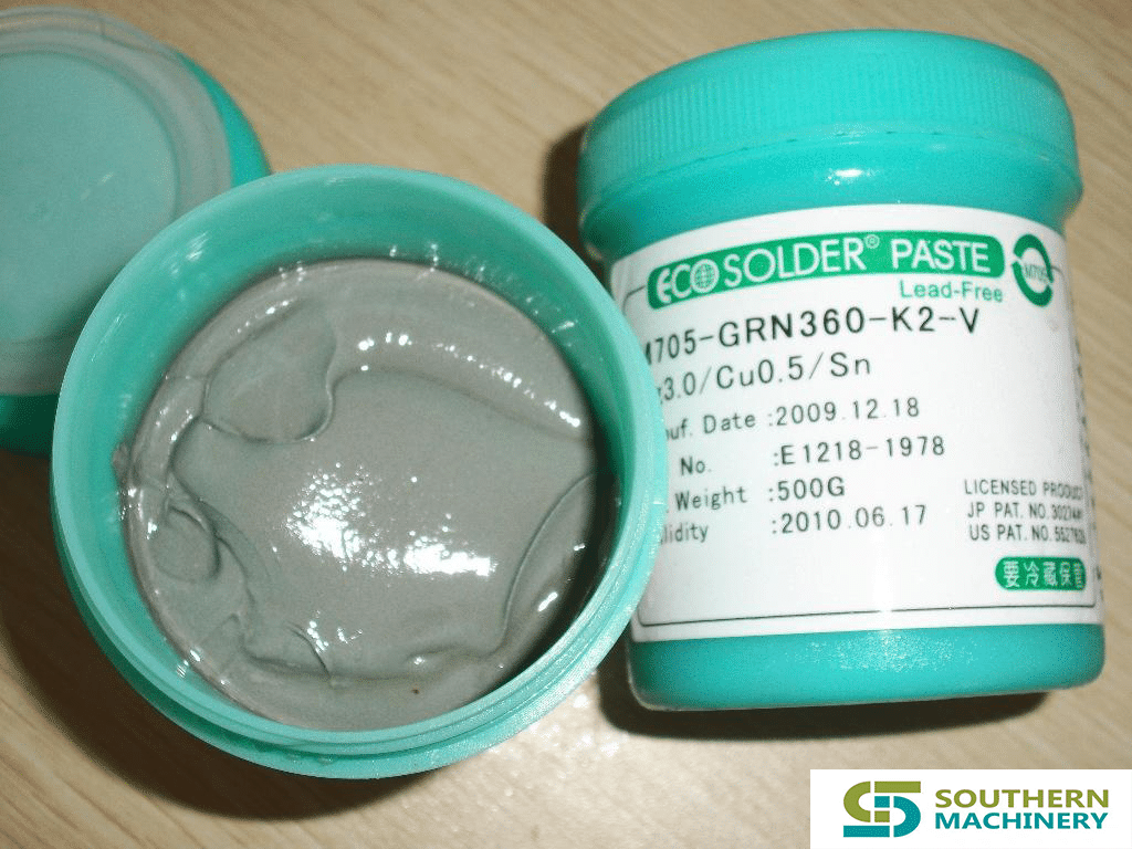
The solder paste itself is a greyish substance consisting of tiny balls of metal, also known as solder. The composition of these tiny metal balls is 96.5% tin, 3% silver and 0.5% copper. The solder paste mixes solder with a flux, which is a chemical designed help the solder melt and bond to a surface. Solder paste appears as a grey paste and must be applied to the board at exactly the right places and in precisely the right amounts.
In a professional PCBA line, a mechanical fixture holds the PCB and solder stencil in place. An applicator then places solder paste on the intended areas in precise amounts. The machine then spreads the paste across the stencil, applying it evenly to every open area. After removing the stencil, the solder paste remains in the intended locations.
After applying the solder paste to the PCB board, the PCBA process moves on to the pick and place machine, a robotic device places surface mount components, or SMDs, on a prepared PCB. SMDs account for most non-connector components on PCBs today. These SMDs are then soldered on to the surface of the board in the next step of PCBA process.
Traditionally, this was a manual process done with a pair of tweezers, in which assemblers had to pick and place components by hand. These days, thankfully, this step is an automated process among PCB manufacturers. This shift occurred largely because machines tend to be more accurate and more consistent than humans. While humans can work quickly, fatigue and eyestrain tends to set in after a few hours working with such small components. Machines work around the clock without such fatigue.Surface Mount Technology | PCBCart
The device starts the pick and place process by picking up a PCB board with a vacuum grip and moving it to the pick and place station. The robot then orients the PCB at the station and begins applying the SMTs to the PCB surface. These components are placed on top of the soldering paste in preprogrammed locations.
Once the solder paste and surface mount components are all in place, they need to remain there. This means the solder paste needs to solidify, adhering components to the board. PCB assembly accomplishes this through a process called “reflow”.
After the pick and place process concludes, the PCB board is transferred to a conveyor belt. This conveyor belt moves through a large reflow oven, which is somewhat like a commercial pizza oven. This oven consists of a series of heaters which gradually heat the board to temperatures around 250 degrees Celsius, or 480 degrees Fahrenheit. This is hot enough to melt the solder in the solder paste.
Once the solder melts, the PCB continues to move through the oven. It passes through a series of cooler heaters, which allows the melted solder to cool and solidify in a controlled manner. This creates a permanent solder joint to connect the SMDs to the PCB.
Many PCBAs require special consideration during reflow, especially for two-sided PCB Assembly. Two-sided PCB assembly need stenciling and reflowing each side separately. First, the side with fewer and smaller parts is stenciled, placed and reflowed, followed by the other side.
Once the surface mount components are soldered in place after the reflow process, which doesn’t stand for completion of PCBA and the assembled board needs to be tested for functionality. Often, movement during the reflow process will result in poor connection quality or a complete lack of a connection. Shorts are also a common side effect of this movement, as misplaced components can sometimes connect portions of the circuit that should not connect.
Checking for these errors and misalignments can involve one of several different inspection methods. The most common inspection methods include:
• Manual Checks: Despite upcoming development trend of automated and smart manufacturing, manual checks are still relied on in PCB assembly process. For smaller batches, an in-person visual inspection by a designer is an effective method to ensure the quality of a PCB after the reflow process. However, this method becomes increasingly impractical and inaccurate as the number of inspected boards increases. Looking at such small components for more than an hour can lead to optical fatigue, resulting in less accurate inspections.
• Automatic Optical Inspection: Automatic optical inspection is a more appropriate inspection method for larger batches of PCBAs. An automatic optical inspection machine, also known as an AOI machine, uses a series of high-powered cameras to “see” PCBs. These cameras are arranged at different angles to view solder connections. Different quality solder connections reflect light in different ways, allowing the AOI to recognize a lower-quality solder. The AOI does this at a very high speed, allowing it to process a high quantity of PCBs in a relatively short time.
• X-ray Inspection: Yet another method of inspection involves x-rays. This is a less common inspection method — it’s used most often for more complex or layered PCBs. The X-ray allows a viewer to see through layers and visualize lower layers to identify any potentially hidden problems.
The fate of a malfunctioning board depends on PCBA company’s standards, they will be sent back to be cleared and reworked, or scrapped.
Whether an inspection finds one of these mistakes or not, the next step of the process is to test the part to make sure it does what it’s supposed to do. This involves testing the PCB connections for quality. Boards requiring programming or calibration require even more steps to test proper functionality.
Such inspections can occur regularly after the reflow process to identify any potential problems. These regular checks can ensure that errors are found and fixed as soon as possible, which helps both the manufacturer and the designer save time, labor and materials.
As a traditional PCB assembly method, thru-hole mounting process is accomplished through collaboration of manual procedure and automatic procedure.
• Step 1: Components Placement – This step is achieved manually by professional engineering staff. Engineers need to quickly, yet precisely place components on corresponding positions based on client’s PCB design files. Component placement must conform to regulations and operation standards of thru-hole mounting process to guarantee high quality end products. For example, they have to clarify polarity and orientation of components, to stop operating component from affecting ambient components, to make completed component placement compatible with corresponding standards and to wear anti-static wristbands when dealing with static-sensitive components like ICs.
• Step 2: Inspection & Rectification – Once component placement is completed, the board is then placed in a matching transport frame where board with components plugged in will be automatically inspected so as to determine whether components are accurately placed. If issues concerning component placement are observed, it’s easy to get them rectified immediately as well. After all, this takes place prior to soldering in PCBA process.
• Step 3: Wave Soldering – Now the THT components should be accurately soldered onto circuit board. In the wave soldering system, the board moves slowly over a wave of liquid solder at high temperature, approximately 500°F. Afterwards, all leads or wires connections can be successfully obtained so that thru-hole components are firmly attached to the board.
Compared with thru-hole mounting process, surface mounting process stands out in terms of manufacturing efficiency because it features a totally automatic mounting PCB assembly process from solder paste printing, pick and place and reflow soldering.
• Step 1: Solder Paste Printing – Solder paste is applied on the board through a solder paste printer. A template ensures that solder paste can be accurately left on correct places where components will be mounted, which is also called stencil or solder screen. Because quality of solder paste printing is directly associated with quality of soldering, PCBA manufacturers focusing on high quality products usually carry out inspections after solder paste printing through a solder paste inspector. This inspection guarantees printing has achieved regulations and standards. If defects are found on solder paste printing, printing has to be reworked or solder paste will be washed off prior to second printing.
• Step 2: Components Mounting – After coming out of solder paste printer, PCB will be auto-sent to pick-and-place machine where components or ICs will be mounted on corresponding pads in the effect of tension of solder paste. Components are mounted on PCB board through component reels in the machine. Similar to film reels, component reels carrying components rotate to provide parts to the machine, which will quickly stick parts to the board.
• Step 3: Reflow Soldering – After every component is placed, the board passes through a 23-foot-long furnace. A temperature of 500°F causes the solder paste to liquefy. Now the SMD components are bound firmly to the board.
Bulk material handle method and process on SMT production line
SMT patch bulk material problems have plagued many SMT people, as we all know, once the placement machine starts, there will definitely be a problem in the SMT production line. For a variety of reasons, many bulk materials are produced, thrown, or are originally bulk materials, or other reasons. Some bulk materials, such as resistors, capacitors, inductors, etc., are not easily distinguishable and have little value in themselves, and there is no value for reuse. However, for large devices, especially some imported chip components, they are of high value and can be distinguished and distinguished, so they are generally reused. However, for scattered components, if the original package is a tray or a suitable tray, the problem may be solved better. Otherwise, it may be more difficult to handle. Southern Machinery today will talk about the handling of bulk material in the SMT production line. Method and process. First, the bulk material handle process
Collecting materials – material personnel sorting materials – using electrostatic bags to pack – paste material specifications – technicians based on bulk material springboard – hand paste bulk material – QC confirmation
Second, the definition
Bulk material: refers to the components that are separated from the original packaging during the production process due to machine throwing, or loading and unloading materials.
Third, job responsibilities
Material staff: responsible for the collection, classification, identification, storage, placement, and placement information of bulk materials, and the material loss rate is calculated according to the order.
QC in front of the furnace: responsible for the manual placement of bulk materials, the front back grain and material code confirmation, PCBA mark, and the classification of bulk materials.
Technician: Responsible for programming, patch production, monitoring patch quality distribution and timely improvement.
QC after the furnace: It is responsible for checking and checking the first piece of all the machines, and the quality is abnormal. Immediate feedback is provided to the front station to improve and track.
Fourth, the work content
In the production process, the material may be thrown due to equipment and other factors, so the operator should check the material step before the patch and after the shift, and check the throwing box and the trash can each time the garbage is dumped. Collect the bulk material and report to the supervisor about excessive bulk material anomalies.
According to the shape of the components, the bulk material is classified according to the shape of the components, and the back code of the components is checked to determine the material code. Then, the checked bulk materials are packed in anti-static bulk box or bulk bag, and the material code identification is performed to confirm the signature of the person. .
When using machine mounting, the operator should first check whether the components are consistent with the normal materials, confirm the material number, and then load the FEEDER tape.
The first piece of material feeding / mid-way refueling, the technician firstly inspects the materials that will be short of materials in the machine half-hour in advance, and collects the materials of the same item number in the component preparation area, and check them correctly, and submit them to the quality department QC/materials. The staff will check again and confirm the total signature of the refueling sheet.