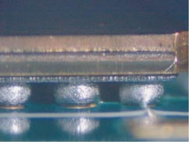
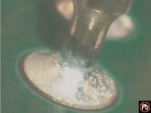
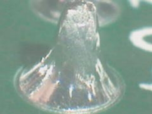
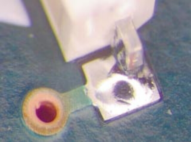
Acceptability for Electronic Assemblies :Soldering Acceptability Requirements

Acceptability for Electronic Assemblies :Soldering Acceptability Requirements


Target-Class1,2,3
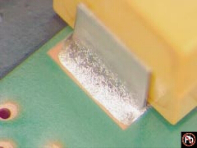
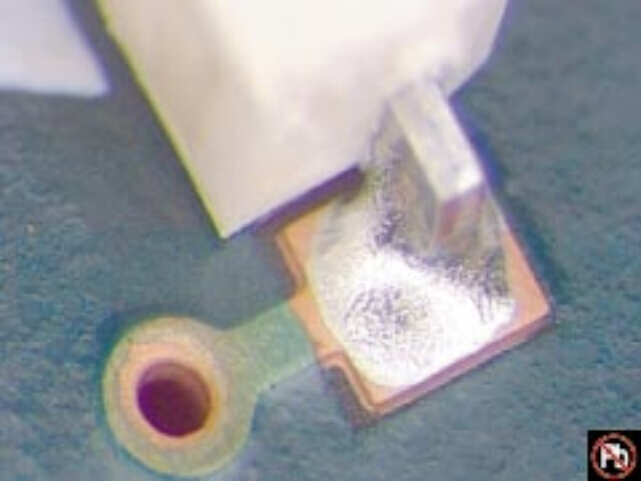
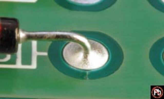
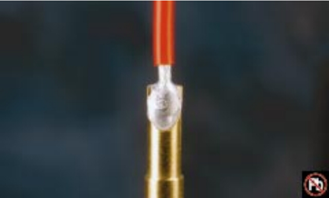
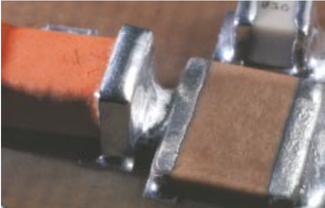
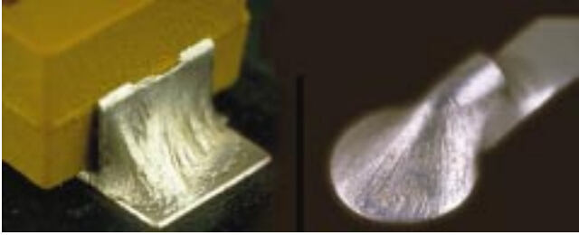
.Solder fillet appears generally smooth and exhibits good wetting of the solder to the parts being joined.
.Outline of the parts is easily determined.
.Solder at the part being joined creates a feathered edge.
.Fillet is concave in shape.


p1s1

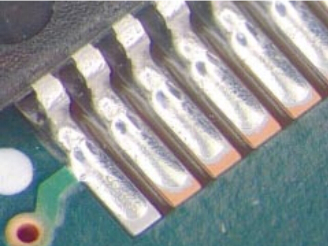
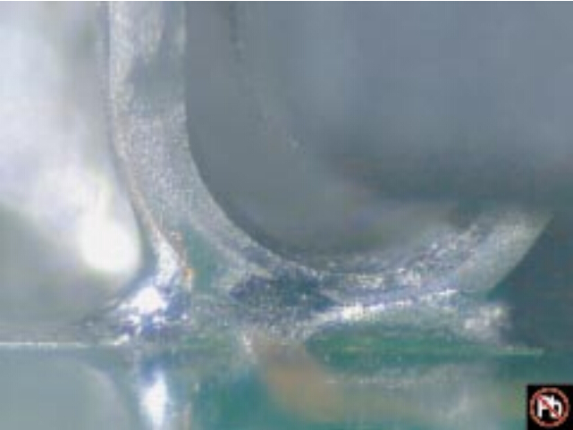
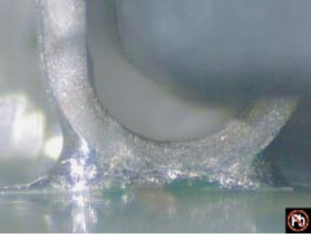
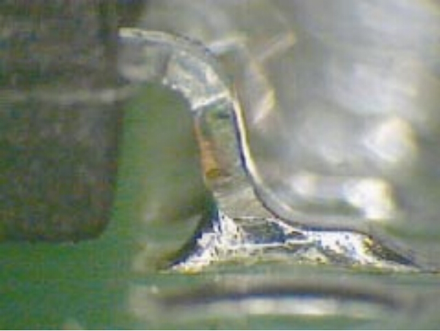
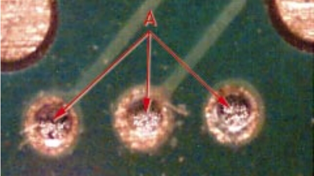
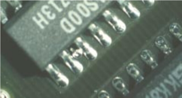
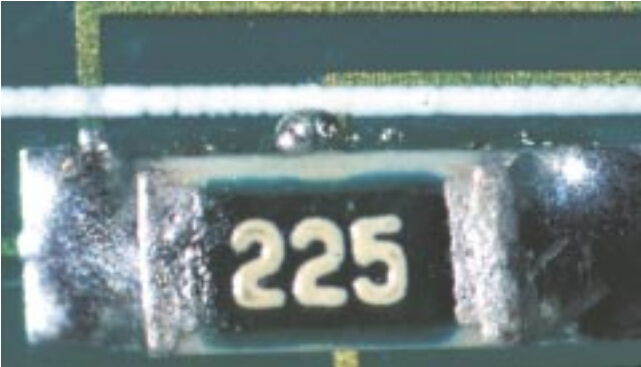
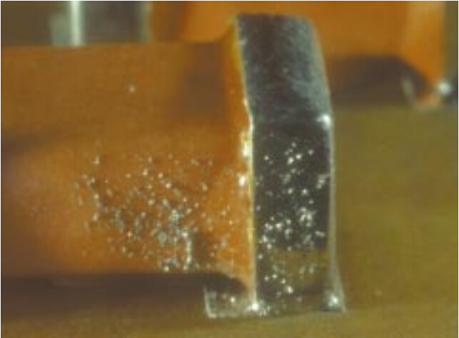
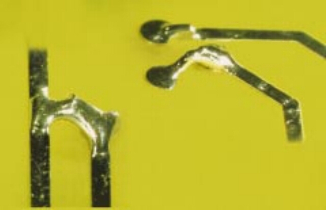
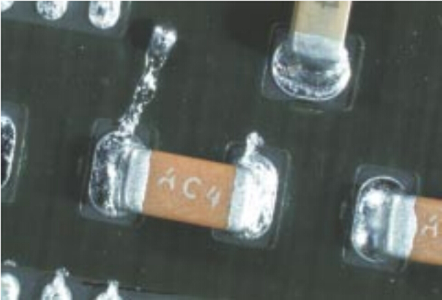
See pic for examples of soldering anomalies.

Acceptable-Class1,2,3
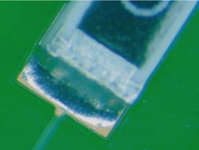
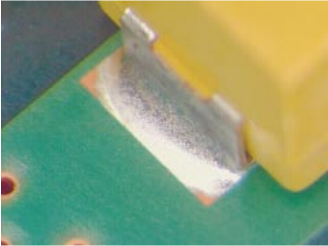
.There are materials and processes,e.g.,lead free alloys and slow cooling with large mass PCBs, that may produce dull
matte,gray,or grainy appearing solders that are normal for the material or process involved.These solder connections
are acceptable.
.The solder connection wetting angle (solder to component and solder to PCB termination do not exceed 90°(Figure).
.As an exception,the solder connection to a termination may exhibit a wetting angle exceeding 90°(Figure)when it is 

created by the solder contour extending over the edge of the solder able termination area or solder resist.


p1s2


Figures below illustrate acceptable solder connections with various solder alloys and process conditions.

p2s1 p2s2

SnPb Solder; No Clean Process                                     SnAgCu Solder;No Clean Process

p2s3 p2s4

    SnPb Solder;Water Soluble Flux                                 SnAgCu Solder;Water Soluble Flux

p2s5 p2s6

   SnPb Solder; Water Soluble Flux                                 SnAgCu Solder;Water Soluble Flux

p3s1 p3s2

     SnAgCu Solder;No Clean Process,N2 Reflow                 SnAgCu Solder,No Clean Process;Air Reflow

p3s3 p3s4

      SnPb Solder;No Clean Process                                  SnAgCu Solder;No Clean Process

p3s5 p3s6

     SnPb Solder;No Clean Process                                   SnAgCu Solder;No Clean Process

p4s1 p4s2

                        SnPb Solder                                                      SnAgCu Solder

p4s3 p4s4

                     SnPb Solder                                                           SnAgCu Solder

p4s5 p4s6

         SnPb Solder ; OSP Finish                                                       SnAgCu Solder; OSP Finish

p5s1 p5s2

                     SnAg CuSolder                                                      SnAg CuSolder

p5s3 p5s4

                 SnAgCu  Solder                                                         SnAgCu Solder


       Soldering Anomalies-Exposed Basis Metal

Exposed basis metal on component leads,conductors or land surfaces from nicks,scratches,or other conditions cannot exceed
there quirements of 7.1.2.3 for leads and 10.2.9.1 for conductors and      lands.
Component leads,sides of land patterns,conductors,and use of liquid photo image able solder resist,can have exposed basis
metal per original designs.
Some printed circuit board and conductor finishes have different wetting characteristics and may exhibit solder wetting only to
specific areas. Exposed basis metal or surface finishes should be considered normal under these circumstances,provided the
achieved wetting characteristics of the solder connection areas are acceptable.


Acceptable-Class 1,2,3
.Exposed basis metal on:
.Vertical conductor edges.
.Cut ends of component leads or wires.
.Organic Solderability Preservative (OSP) coated lands.
.Exposed surface finishes that are not part of the required solder fillet  area.

p6s1 p7s1


Acceptable-Class 1

Process Indicator-Class 2,3

.Exposed basis metal on component leads,conductors or land surfaces from nicks or scratches provided conditions

do not exceed the requirements of7.1.2.3 for leads and 10.2.9.1 for conductors and lands.

p7s2


 Soldering Anomalies-Pin Holes/Blow Holes


Acceptable-Class1
ProcessIndicator-Class2,3

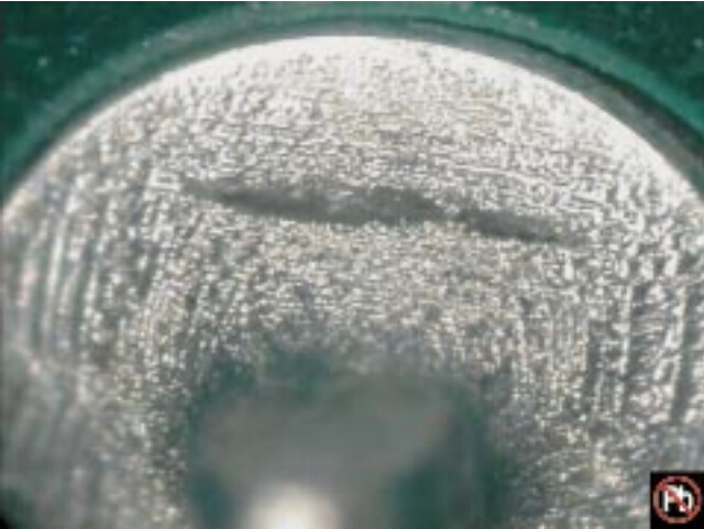
.Blowholes (Figures 1,2),pinholes (Figure 3),voids (Figures 4,5),etc.,providing the solder connection meets all other requirements.


p8s1 p8s2                           

                          1                                                                                2                                                                        

p8s3 p8s4

                             3                                                                                 4

 p8s5                     

                                  5

Defect-Class 2,3

Solder connections where pin holes,blowholes,voids,etc.
reduce the connections below minimum requirements(not shown).


Soldering Anomalies-Reflow of Solder Paste

 Defect-Class1,2,3
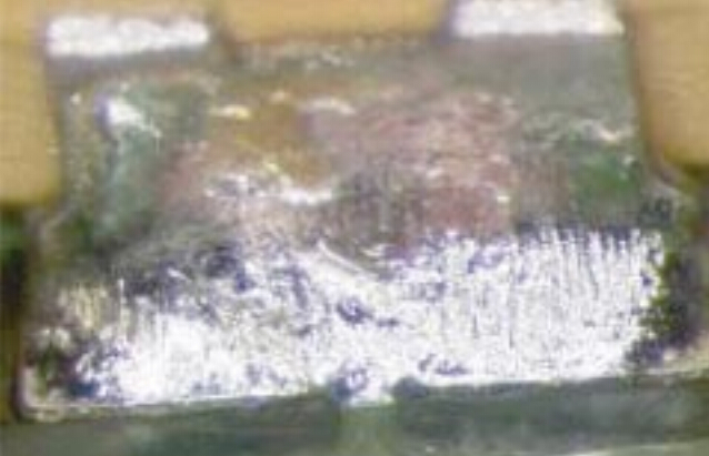
.Incomplete reflow of solder paste.


p9s1

 p9s2


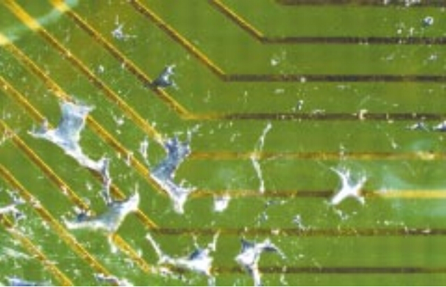
Soldering Anomalies-Nonwetting

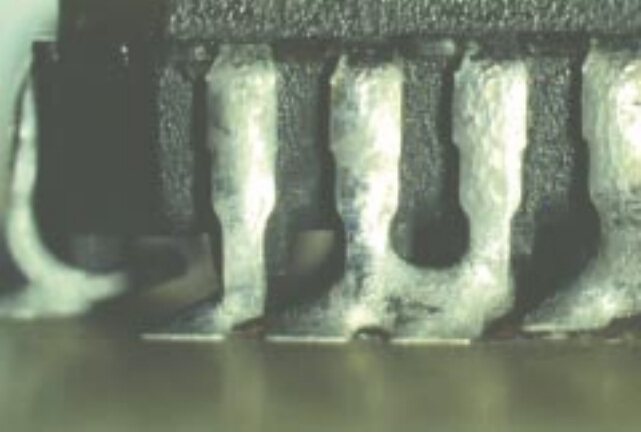
IPC-T-50 defines nonwetting as the inability of molten solder to form a metallic bond with the basis metal.In this Standard,that
includes surface finishes.

Defect-Class 1,2,3
.Solder has not wetted to the land or termination where solder is required.
.Solder coverage does not meet requirements for this termination type.

p10s1

p10s2

p10s3

p10s4

p10s5


Soldering Anomalies-Dewetting

Defect-Class 1,2,3
.Evidence of dewetting that causes the solder connection to not meet the SMT and thru-hole solder fillet requirements.


p11s1

p11s2

p11s3


                          Soldering Anomalies-Excess Solder-Solder Balls/Solder Fines

Solder balls are spheres of solder that remain after the soldering process.Solder fines are typically small balls of the original 

solder paste metal screen size that have splattered around the connection during there flow process.


Target-Class 1,2, 3
.No evidence of solder balls on the printed wiring assembly.

p12s1

Acceptable-Class 1,2,3
.Solder balls are entrapped/encapsulated and do not violate minimum electrical clearance.
 Note:Entrapped/encapsulated/attached is intended to mean that normal service environment of the product will not cause a solder ball to become dislodged.

p12s2


Defect- Class 1,2,3
.Solder balls violate minimum electrical clearance.
.Solder balls are not entrapped in no-clean residue or encapsulated with conformal coating,

or not attached(soldered)to a metal surface.

p13s1

p13s2

p13s3

p13s4


Soldering Anomalies-Excess Solder-Bridging


Defect-Class 1,2,3
.A solder connection across conductors that should not be joined.
.Solder has bridged to adjacent noncommon conductoror component.

p14s1

p14s2

p14s3

p14s4


Soldering Anomalies-Excess Solder-Solder Webbing/Splashes

Defect-Class 1,2,3
.Solder splashes/webbing.


p15s1

p15s2


Soldering Anomalies-Disturbed Solder

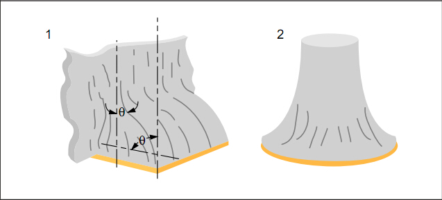
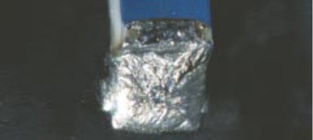
Surface appearance with cooling lines as shown in Acceptable pic is more likely to occur in lead free alloys and is not a disturbed solder condition.

p16s1


Defect-Class 1,2,3
Characterized by stress lines from movement in the connection (SnPb alloy).

p16s2

p16s3

p16s4

p16s5


Soldering Anomalies-Fractured Solder


Defect-Class 1,2,3
Fractured or cracked solder.


p17s1

p17s2


Soldering Anomalies-Solder Projections

Defect-Class 1,2,3
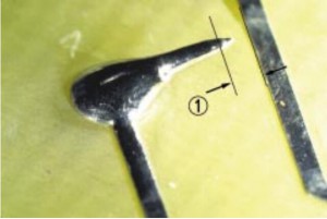
.Solder projection,figure 1,violates assembly maximum
height requirements or lead protrusion requirements.
.Projection,figure 2,violates minimum electrical clearance(1).


p18s1 p18s2

                       1                                                              2


p18s3


Soldering Anomalies-Lead Free Fillet Lift

Acceptable-Class 1,2.3
.Fillet lifting-separation of the bottom of the solder and the
top of the land(primary side of plated-through hold connection).

Process Indicator-Class 2
Defect-Class3

.Fillet lifting-separation of the bottom of the solder and the top of the land(secondary side of plated-through hold connection)(not shown).
Defect-Class 1,2,3
.Fillet lifting damages the land attachment.

p19s1


Soldering Anomalies-Hot Tear/Shrink Hole

Acceptable-Class1,2,3
.For connections made with lead free alloys:
.The bottom of the tear is visible.
.The tear or shrink hole does not contact the lead,land or
barrel wall.


Defect-Class 1,2,3
.Shrink holes or hot tear in connections made with SnPb  
solder alloys:

.For connections made with lead free alloys:
.The bottom of the shrink hole or hot tear is not visible.
.The tear or shrink hole contacts the lead or land.

p20s1

                                   end

FREQUENTLY ASKED S-K100 High Speed LED PICK & PLACE MACHINE QUESTIONS AND ANSWERS

1)What is high speed led tube and led strip pick and place machine ?

The high speed automatic SMT mounting machine is the equipment used to realize high-speed, high accuracy completely automatic mounting the electric elements like LED light sphere, electric resistance , electric capacity etc. It is the mot essential and most complex equipment in the entire SMT production. The mounting machine is the major machine in SMT production line, and it is already developed from the early low speed mechanical mounting machine to high-speed optics mounting machine, and to multipurpose, flexible connection modulation development.


2)What machines does the LED PCB board assembly need ?

The LED mount technical process simplification is: Printing, Pick and placing, Soldering, Overhaul (in each part, you can join examine link to control quality)


3) What are the advantages of Langke smd pick and place machine?

A.Top high speed in the world, quicker than the main SMT pick and place machines brands like Siemens, Fuji, Samsung, Panasonic, Sanyo and Juki led pcb pick and place machines;

B.Lowest power consumption, 2.5-3.5KW/Hour, our machine has the smallest electricity consumption among the high speed pcb pick and place machine manufacturers in China

C.Match vacuum pumps along with the main machine, no need to match extra vacuum pump;

D.Electric control system is installed on the top of the main machine, easy to maintain, and has a good damp proof effect;

E.Integrated forming steel frame, guarantee stable performance on high speed running conditions.

F.The distance of sucking mouth can be adjusted manually, photoelectric will make sure the accuracy after adjust, allow you to mount different pitches PCB board.


4) What kinds electric components can use our automatic led smt pick and place assembling machine!

The main elements our machine can mount include: LED lights, electric capacity and electric resistance, sizes like: 0805,1206,2121,2835,3014,3528,5050,5630,5730,RGB; mainly for 1.2-1.5 meter LED light tube, LED panel light, 0.5-1.0 meter LED light strip , RGB strip.

Debugger reference manual for SMT machine Radysis Motion Controler

UBUG Users Guide ( Debugger reference manual )

for Radysis Motion Controler


 The
UBUG monitor is a stand alone software package designed to allow
evaluation and debugging of the UIMC 68EC030 based motion controller
PCB. It has the capability to load and execute user code and includes
an assembler/disassembler designed for quick program patchwork. The
monitor operates in a user interactive command driven mode signified by
the UIC> prompt. The command line entered after this prompt
determines which operation is performed.


         UBUG MONITOR


TABLE OF CONTENTS


1. GENERAL INFORMATION  

         1.1  Description of UBUG…………………..  3


2. THE UBUG COMMAND SET

         2.1  Introduction…………………………    3

         2.2  Auto Null (an)………………………    4

         2.3  Assembler/Disassembler (as) …………..  4

         2.4  Block of Memory Fill (bf)……………..  6

         2.5  Block of Memory Move (bm)……………..  6

         2.6  Break Point (br)……………………..    6

         2.7  Block Search (bs)…………………….    7

         2.8  Counter Test (ct)……………….      7

         2.9  DAC16, ADC8 Test (dac16t)…………….  7

         2.10  Data Conversion (dc)………………….  8

         2.11  Go (go)……………………………..    8

         2.12  Help (?/he/help)……………………..    8

         2.13  IO Access (io)………………..      8

         2.14  Load S-Records (lo)…………………..  9

         2.15  Memory Display (md)…………………..  9

         2.16  Memory Modify (mm)……………………  10

         2.17  Memory Test (mt)…………………..    10

         2.18  Register Display (rd)…………………    10

         2.19  Register Modify (rm)………………….  11

         2.20  Symbol Define (sd)……………………  11

         2.21  Test – Diagnostic (test)……………….    11

         2.22  Transparent Mode ™…………………  12

         2.23  Trace (tr)…………………………..    12


3 USING THE ONE-LINE ASSEMBLER/DISASSEMBLER

         3.1  Introduction ……………………….    12

         3.2  Entering and Modifying Source Program ….  12

       
 3.3  Entering a Source Line………………..  13          
 3.4  Entering a Change of Flow Instr ………  14

       
 3.5  Entering Register Lists ………………  15          
 3.6  Entering Floating Point Immediate Data …  16          
 3.7  Entering MMU Instructions …………….  17


1.  GENERAL INFORMATION


1.1  DESCRIPTION OF UBUG

 The
UBUG monitor is a stand alone software package designed to allow
evaluation and debugging of the UIMC 68EC030 based motion controller
PCB. It has the capability to load and execute user code and includes
an assembler/disassembler designed for quick program patchwork. The
monitor operates in a user interactive command driven mode signified by
the UIC> prompt. The command line entered after this prompt
determines which operation is performed.


2.  THE UBUG COMMAND SET


 2.1  INTRODUCTION

 This
section explains the UBUG monitor commands and their associated syntax.
Table 2.1 summarizes the available commands and shows the section where
the command is explained in greater detail.


TABLE 2.1 UBUG MONITOR COMMANDS


Command/Mnemonic

Name

Section

an

Auto Null

2.2

as

Assembler/Disassembler

2.3

bf

Block of Memory Fill

2.4

bm

Block of Memory Move

2.5

br

Breakpoint

2.6

bs

Block of Memory Search

2.7

ct

Counter Test

2.8

dac16t

DAC16, ADC8 Test

2.9

dc

Data Conversion

2.10.

go

Go

2.11

?/he/help

Help

2.12

io

IO Access

2.13

lo

Load S-Records

2.14

md

Memory Display

2.15

mm

Memory Modify

2.16

mt

Memory Test

2.17

rd

Register Display

2.18

rm

Register Modify

2.19

sd

Symbol Define

2.20.

test

Test – Diagnostic

2.21

tm

Transparent Mode

2.22

tr

Trace

2.23


 The command line is composed of:

 <COMMAND IDENTIFIER>: specifies which command (ex. br )

 <SP>:   at least one space

  OPTION LIST: an option may use delimiter(-) with options if non-default
options    are allowed and are being used. (ex.
[<-r>])

  <SP>: at least one space

  ARGUMENTS: any required arguments specified by the command separated
    by commas/spaces as shown in the command
description. (ex. <ADDR,ADDR>)


 where “<>” enclose symbols that are required on the command line
and “[<>]” enclose symbols that are optional on the command
line. Note, in the above examples the -r option was an example of an
optional symbol and that the ADDR fields are requirements on the
command line. The options available with a given command are fully
explained in the section that describes that command. The monitor is
not case sensitive to input from the terminal. All input from the
terminal is converted to lower case before being used internally (except
text following a text delimiter; See TEXT below). The arguments of a
given command are described using the following symbols:


 <EXP>: An expression can be any numerical expression which may
be evaluated using only the arithmetic + and – operators.

 Ex. 1000

    Ex. 1+3


 Note: Numbers may be preceded with a base designator if the default
(hexadecimal) is not desired. These designators are shown below in Table
2.2:


TABLE 2.2 BASE DESIGNATORS

Base

Designator

Hexadecimal

$

Decimal

&

Octal

@

Binary

%


 <ADDR>: Address field is any valid expression. Note: This
address field should not be      confused with the source and
destination addresses required using the        Assembler/Disassembler.


  <COUNT>: Count field is any valid expression preceded by a COUNTDEL (count      delimiter ie. “:”)

 Ex. :100


 <RANGE>: A range of memory locations denoted by either ADDR,ADDR or        ADDR:COUNT.

 Ex. 0,100

    Ex. 0:50


  <TEXT>: An ASCII string of up to 255 characters preceded by a TEXTDEL (text    delimiter i.e.. “;”)

 Ex. ;sample text


  <SIZE>: Can be either:

    byte (8 bit)  ====> -b

    word (16 bit  )  ====> -w

    long (32 bit)  ====> -l

**Note: ====> stands for “is represented by” or “returns”


 <DATA>: Data can be any valid expression.


  <MASK>: A mask may be any expression. After evaluating the
expression 0’s      represent don’t cares. A mask is sometimes
used to qualify


 <DATA>. See section 2.6 for an example of usage.


2.2  AUTO NULL

 an <AXIS>


 The auto null function performs a nulling of the zero offset of the 16bit DAC of the axis specified.


 Examples of use:

 an 1    ( nulls axis one )


2.3   ASSEMBLER/DISASSEMBLER

 as <ADDR>


 The assembler/disassembler is invoked at the address given and
disassembles the object code at that location. Use of the
Assembler/Disassembler is fully described in chapter 3.


2.4   BLOCK OF MEMORY FILL

 bf [<SIZE>] <RANGE> <DATA>


 The block fill command fills the specified range of memory with the
data listed. If the size option is not specified the default size used
is word. If a multiple of the <SIZE> of <DATA> does not
fit evenly in the <RANGE> the command leaves the last partial
word or long word unchanged.

 Examples of use:

         bf 100,110  &10

  bf 100:8    &10

 bf -w 100:8   a

 bf -l 100,110    a000a

**Note: All of these examples perform the same memory fill.

        (ie. $00000100: $000a $000a $000a $000a $000a $000a

 $0000010C: $000a $000a $0000 $0000 $0000 $0000 )


2.5   BLOCK OF MEMORY MOVE

 bm [<SIZE>] <RANGE> <ADDR>


 The block move command allows the user to copy segments of memory to
different locations in memory. The execution of this command does not
destroy the original version unless the location moved to <ADDR>
is within the range <RANGE> of the code being copied. The size
option is only available when range is described as
<ADDR>:<COUNT> . If range is being described with the
<ADDR>,<ADDR> mode the size defaults to byte. The size
field represents the size transfer that is used to accomplish the memory
move.


         Examples of use:

         bm 1000,2000   10000

 bm 1000:800  10000

 bm -l 1000:400  10000 **Note: This variation executes the fastest

**Note: All of these examples perform the same memory move.


2.6   BREAKPOINT

  br

  br <ADDR>

  br <ADDR> <:COUNT>

  br -r [<ADDR>]

 br -r


 The breakpoint command allows the user to list, insert or delete
breakpoints in the target code. This allows the user to stop executing a
program and return to the monitor environment when the specified
<ADDR> is prefetched. The different uses of this command are
summarized below:


         br    list all known breakpoints

 br <ADDR>     insert a breakpoint at this address

 br <ADDR> <:COUNT>  insert a breakpoint at this address, however, return to the             monitor environment only after encountering the
       breakpoint <COUNT> number of times.

  br -r [<ADDR>]  remove the breakpoint at this address

  br -r    remove all breakpoints


2.7   BLOCK SEARCH

  bs [<SIZE>] <RANGE> <DATA>

 bs [<SIZE>] <RANGE> <DATA> <MASK>


 The block search command allows the user to find a specific pattern
within memory. The search area may extend beyond the <RANGE>
specified if a pattern is started within <RANGE>. There are two
primary types of searches:


 bs [<SIZE>] <RANGE> <DATA>  searches the range for an exact match of                <DATA>.

  bs [<SIZE>] <RANGE> <DATA> <MASK> searches
the range for any pattern that                matches <DATA>
where there is a “1” in                the binary representation of the
mask.


 Ex. With memory at location $100 as shown below, executing

 “bs 100,118 $1234 $ffbf” ====>  

         Starting address: $00000100

         Ending address: $00000117

         Found at: $00000110:$1234

         Found at: $00000114:$1274

 Memory for the example above:

$00000100: $0000 $0000 $0000 $0000 $0000 $0000

 $0000010C: $0000 $0000 $1234 $0000 $1274 $0000


2.8  COUNTER TEST

 ct


 The counter test command performs a diagnostic test on the 4 axis counters and pass/fail information is returned.


2.9  DAC16, DAC8 TEST

 dac16t <AXIS #>


 The dac16t command performs a diagnostic test of the 16bit DAC and the
8 bit ADC for the axis specified by using the diagnostic wrap around
capability of the UIMC. Pass/fail information is returned.


2.10  DATA CONVERSION

 dc <EXP>


 The data conversion command allows the user to evaluate an input
expression and determine its hexadecimal and decimal equivalent.


 Examples of use:

 **NOTE:  The following symbols have been defined earlier in order

     to be used in the examples below:

     Ex 1. uses   /start= 0

     Ex 2. uses   /start= – $18

     Ex 3. uses  /finish= 10000 and /start=$10000

     (see section 2.17 )

          Ex. 1 dc $17+/start ====>  $17 = &23  

  Ex. 2 dc $17+/start ====>  UNSIGNED : $FFFFFFFF =
&4294967295           SIGNED
: -$1 = -&1

 Ex. 3 dc $/finish-/start ====>  $10000 = 65536


2.11   GO go [<ADDR>]


 The go command allows the user to execute target programs. If an
address is not specified on the command line then the current PC value
is used. This value is either:

 1.) the initialized PC value if no target code has been run.

 2.) the last value of the PC used in executing target code.

 3.) the value placed into the PC register by a RM command (Register Modify see section    2.16 ).

 If an address is included on the command line then the PC is modified
to be the specified addr. and execution begins at this address. In
both cases, the register state that the microprocessor is initialized
to, before executing the target code at this location, can be viewed by
executing a rd command (See section 2.15).


2.12   HELP

  ? [<symbol>]

  he [<symbol>]

 help [<symbol>]


 The help command allows the user to view a list of allowable commands
and the syntax associated with them. Symbols used to describe the
command usage can be looked up also.

 Examples of use:

 ?,he or help  ====> return a complete listing of all commands with usage

  ? as  ====> AS <addr> help addr ====> <number>

 he number  ====> <hex> || <dec> || <oct> || <bin> || <symbol>

** Note: <number> may also be an expression


2.13  IO ACCESS

 io


 The IO access command allows the user to access various options of the
UIMC motion controller. Upon issue of the IO command the user will be
presented with the following list of choices:

 I/O Interface Menu:

  i – View Inputs ( Debugger displays current state of the digital inputs)

 o – Modify Outputs  ( Debugger allows user to modify outputs)

 c – Modify Counters  ( Debugger displays current state of counters and allows user to          modify the contents )

 r – Modify Relays  ( Debugger allows user to modify the state of the relays )

 x – Modify 16bit DACs ( Debugger allows user to modify the 16bit DAC outputs )

 y – Modify 8bit DACs   ( Debugger allows user to modify the 8bit DAC
outputs )       z – View 8bit ADCs ( Debugger displays current state of
ADCs )


After selection of one of the above the user will be prompted appropriately.


2.14 LOAD S-RECORD

 lo [<port>] [<OFFSET>] ;<TEXT>


 The load command allows the user to download S-Records from the host
system. If an offset is present on the command line then the target
address is the offset added to the address determined by the S-Record.
In normal mode the command sends the <TEXT> beyond the “;” to the
HOST. It then expects the HOST to begin sending S-Records to the
terminal. If the ‘t’ option is used no ; is necessary and the debugger
expects the terminal to begin sending an S-Record.

 Examples of use:

          lo ;cat ubug.mx

**Note:  The “cat” command is a UNIX command that concatenates
and then prints      the specified files using standard output.
This effectively sends the contents of the    file to the terminal. The
monitor then loads the contents of the S-Records in the      file to
the addresses determined by the S-Records via the Host port.

.


          lo a0000 ;cat ubug.mx

**Note:  This command downloads the same S-Record file used in
the first example except  that it is down loaded into memory at the
address determined by the S-Record + $a0000    (i.e.. the offset is
added in).


 lo t

**Note:  This command uses ‘t’ for terminal for the S-Record load port.


2.15   MEMORY DISPLAY

  md [<SIZE>] <addr>

  md [<SIZE>] <RANGE>

 md -di <addr>


 The memory display command allows the user to view memory. The size
used to display the memory is determined by the size option. If no
option is used the default is word. If the range exceeds the screen
capacity, output to the screen is suspended until any key is pressed.


  Examples of use:

 md -l 100,110

  md -l 100:4

  md 100:8

 md -di 100  

**Note: This command begins to disassemble the memory at

  this location.


2.16 MEMORY MODIFY

  mm [<SIZE>] [<verify>] <ADDR>

 mm <CONTROL>


 The memory modify command allows the user to view and modify memory.
The size used to display the memory is determined by the size option.
The size default is word. The write only option is determined by the
verify option. The default is read/write and an ‘n’ is used for write
only. Memory is displayed beginning at the address specified followed
by a ‘?’ prompt. The user may type in an <exp> to replace that
memory value or hit return to view the next memory value. To exit the
command, type “. <cr>” (period <carriage return>). Other
available <CONTROL> characters are summarized below in Table 2.3:

TABLE 2.3 CONTROL CHARACTERS

Control Character   Designator

– <EXP>  backup     <EXP> memory locations

+ <EXP>  advance      ” ”  “

= <NUMBER>  do not advance  Will not advance to next memory location


         Examples of use:

 mm -l 100  ====>  $00000100 $00000000 ?

 mm 100  ====>      $00000100 $0000 ?

 (i.e.. uses the default “word” size)

 mm n 100  ====>    $00000100 ?

 (i.e.. does not read from location)


2.17  MEMORY TEST

 mt <start> <finish>


 The memory test performs a bit by bit memory test on the range of RAM specified and pass/fail information is returned.


2.18   REGISTER DISPLAY

 rd

 rd -f Note: Coprocessor registers displayed if present


 The register display command allows the user to view the contents of the registers of the mpu/fpu.


2.19   REGISTER MODIFY

 rm [<REGISTER> [<New Value>]]


 The RM command allows the user to the modify the contents of the registers of the mpu.

 Examples of use:

 To change the PC value:

 rm pc 3000  ====>  changes the PC value to 3000

or

 rm  ====>  Which register?

     pc  ====>   PC=00004000NEW VALUE?

       3000  ====>  changes the PC value to 3000

or

 rm pc  ====>  PC=00004000NEW VALUE?

      3000 ====> changes the PC value to 3000


2.20   SYMBOL DEFINE

  sd [<SYMBOL> <EXP>]

 sd -r <SYMBOL>


 The symbol define command allows the user to define symbols. These
symbols can then be used within expressions. Using a symbol in an
expression results in the symbol being substituted with the expression
that was used to define it. Once defined, the symbol is available
until the monitor is reset. If a symbol is defined multiple times the
monitor uses the first definition.


         Examples of use:

 sd ====> lists which symbols are already known

  sd /reset 10000 ====> defines /reset to be $10000 whenever it is
used in an expression.  sd /start -$18 ====> defines
/start to be -$18 whenever it is used in an expression.    sd -r
/start ====> removes the first definition of /start from the
list

**NOTE: Symbols that have been defined using the sd command
can be used in any    expressions. An example of this is to use a
symbol defined to enter source code while in  the
assembler (i.e.. bsr /startsub after defining /startsub).


2.21  TEST – DIAGNOSTIC

 test [<LOOP #>]


 The test command initiates a series of diagnostic test consisting of
an auto null function, counter test, RAM test, and DAC16/ADC8 test and
returns pass/fail information. The number of times the diagnostic test
are performed is determined by the loop # specified. If no loop # is
specified the command cycles infinitely.


2.22  TRANSPARENT MODE

 tm


 The transparent mode command places the user into transparent mode by
establishing a software connection between the HOST and TERMINAL.
Transparent mode preempts normal communication between the TERMINAL and
the debugger. While in this mode all keyboard input is relayed directly
to the HOST. HOST responses, in turn, are returned to the screen.
Typing a CTRL A returns the user to the monitor environment.


2.23   TRACE

 tr [<ADDR>][<COUNT>]


 The trace command allows the user to trace though target code and
observe the registers after executing the command line. If count is
specified then the microprocessor executes <COUNT> number of
instructions before returning to the monitor environment. Trace begins
from the <ADDR> listed on the command line or from the current PC
if an <ADDR> is not included. The trace instruction can be
continued by hitting a carriage return. To exit, a “.” must be entered.


         Examples of use:

          tr   ====> traces 1 instruction from the current PC

 tr :10   ====> executes 10 instructions past the current PC then returns to
the monitor   environment

 tr 1000====> traces 1 instruction starting at $1000


3.0  USING THE ONE-LINE ASSEMBLER/DISASSEMBLER


3.1 INTRODUCTION

 Included in the UBUG monitor is an assembler/disassembler command
which can be executed as detailed in the previous section. This
assembler/disassembler allows the user to modify target code. Each
source line that is typed in by the user is entered into memory at the
displayed address. This line is then disassembled so that the user can
verify the actual code entered into memory. If no change is desired a
<CR> moves the user to the next opcode in memory.

 CAUTION: This assembler/disassembler does not insert code into the
source program; it merely overwrites memory at that location. As a
result, a program patch that requires code insertion can be accomplished
by first Block Moving code to free up an insertion area and then
inserting into that area.


3.2 ENTERING AND MODIFYING SOURCE PROGRAM

 In order to enter and modify source code, the as command should be
executed as detailed in section 2.2 (i.e.. as <ADDR>). This
places the user into the Assembler/Disassembler routine.

Table 3.1 summarizes the commands that can be executed within this routine:

TABLE 3.1 ASSEMBLER/DISASSEMBLER SUB COMMANDS

Command    Designator

BACKUP <EXP>  – <EXP>

ADVANCE <EXP>  + <EXP>

FINISH  .

HELP  ?

STEP PAST    carriage return

DEFINE CONSTANT  DC #<EXP>


**Note: Executing a ‘?’ while in the assembler/disassembler returns
the DEVICE that the assembler/disassembler is supporting.


3.3 ENTERING A SOURCE LINE

 After executing an as <ADDR> command, the assembler/disassembler
returns with the disassembly of the code found at that location. At
this time the user may execute an assembler command shown in section 3.2
or type in the source line that is to replace the displayed source
code. While entering source the standard MOTOROLA effective addressing
modes are used. These modes are summarized below in Table 3.2:


TABLE 3.2 ASSEMBLER/DISASSEMBLER EFFECTIVE ADDRESSING MODES


Effective Addressing Mode      Syntax

Register Direct      Dn

Address register direct      An

Address register indirect      (An)

Address register indirect with Postincrement  (An)+

Address register indirect with Predecrement  -(An)

Address register indirect with Displacement  (d16,An)

Address register indirect with Index (d8)  (d8,An,Xn.SIZE*SCALE)

Address register indirect with Index (base disp)  (bd,An,Xn.SIZE*SCALE)

Memory indirect Post-indexed    ([bd,An],Xn.SIZE*SCALE,od)

Memory indirect Pre-indexed    ([bd,An,Xn.SIZE*SCALE],od)

PC indirect with displacement    (d16,PC)

PC indirect with index (d8)    (d8,PC,Xn.SIZE*SCALE)

PC indirect with index (bd)    (bd,PC,Xn.SIZE*SCALE)

PC memory indirect Post-indexed    ([bd,PC],Xn.SIZE*SCALE,od)

PC memory indirect Pre-indexed  
 ([bd,PC,Xn.SIZE*SCALE],od) Absolute Short Address
       (xxx).W

Absolute Long Address    (xxx).L

Absolute Address    xxx optimizes (bwl)

Immediate Data      #xxx


 While using the POST or PRE indexed modes, fields may be skipped by using a comma. An example is shown below:

 Ex.  andi #12,([,],,)  ====>  andi.b  #$12,([$0,ZA0],ZD0.W*1,$0)


Other examples of source lines are shown below:

        Ex.  ori.l #12,(a1)  ====>  ori.l #$12,(a1)

 Ex.  addq #1,(a1)  ====>  addq.b #$1,(a1)


 There are only limited error screening abilities included within the monitor. Examples of this are shown below:

 Ex.  jmp (123).w  ====>  jmp ($123).W

**Note:  When executed results in a bus error.


 Ex.  bsr (123)  ====>

 ERROR 10:illegal change of flow ===> bsr (123)

     Note:  The bsr instruction does check for illegal

           changes of flow.

 NOTE:  Flow may not be changed to an odd addr.

 Upper digits of data are NOT truncated when a mismatch between size
and immediate data is found if the byte or word size option was
specifically entered. If the long size option is specified and data
exceeds this range then upper digits ARE truncated.


 Ex.  addi.b #12345678,(a1) ====>

 ERROR 11:immediate data/size option error ===> addi.b #12345678,(a1)


 Ex.  addi.l #123456789,(a1) ====> addi.l #$23456789,(a1)

 Ex.  addi #123456789,(a1) ====> addi.l #$23456789,(a1)

   (defaults to the long option)

      truncated————–^


 Upper digits of data are truncated on commands that have a limited
field in the opword to store the immediate data. Examples of this are
shown below.

 Ex. addq #10,(d0)  =====>  addq.b #$0,(d0)

 Ex. trap #10  =====>  trap #$0 input is hex default

 Ex. trap #&10  =====>  trap #$A


3.4 ENTERING CHANGE OF FLOW INSTRUCTIONS

 Since the assembler/disassembler does not use labels, all instructions
that use <label> as an effective addressing mode must have their
displacement determined. If initially unknown, space for this
displacement must be reserved and then the user needs to come back and
enter the displacement. Once the displacement has been determined it
may be entered as shown in the following example:


 Ex. In this example the location of the target instruction of a branch
is known to be $100000 and a BRA is needed at location 0. After
executing “AS 0” and obtaining the disassembly found at 0 the user
could type:

  BRA 100000 or BRA (100000) or BRA.l #ffffe


 The absolute addressing mode can be used if the target address of a
branch is known (as in the first 2 examples) or the displacement (last
example) can be entered using the immediate data addressing mode.


   CAUTION:  In some instances unexpected results can occur while using

 change of flow statements. These instances are summarized below

 with examples.


Ex.
1 If the degenerate case of a branch statement is used (i.e..
attempting to use a short branch to branch to the following instruction)
the assembler mistakenly assembles this .b option. However, since the
displacement is zero this is a .w opcode and the disassembler correctly
displays this fact to the user.


  $00004000 nop ? bra.b ====> results in an INCORRECT assembly


 Ex. 2 If the user attempts to force a particular size branch
statement and the actual branch requires a greater displacement than was
reserved then the assembler prints an error message: “ERR0R 16: OUT OF
DISPLACEMENT RANGE” .


 $00004000 nop ?bra.w (100000)


One
way to assure this does not occur is to not enter a size option. This
allows the assembler to choose the correct size for the displacement.


3.5 ENTERING REGISTERS and REGISTER LISTS

 The move multiple register instruction (movem) uses a register list as
an effective address. This list may be entered in the following
method:


 Ex.  a0    ====> single address register

   d3    ====> single data register

   a0-a3     ====> series of registers

   a0-a3/a7  ====> combination of previous examples

   a0-a7/d0-d7  ====> all of the registers


 If coprocessor support is specified then the floating point registers

can be entered as shown below:


 Ex.   fp0  ====> single floating point register

   fp0-fp2   ====> series of registers

   fp0-fp3/fp7  ====> combination of previous examples


 Many of the commands require the entering of registers other than data
or address registers. Tables 3.3 show listings of the registers that
are used and the abbreviations accepted by the assembler:


TABLE 3.3 68030 REGISTERS ( MMU Registers not availiable on 68EC030 )

Name    Syntax  

User Stack Pointer  USP

Status Register  SR

Condition Code Register  CCR

Program Counter  PC

Master Stack Pointer  MSP

Interrupt Stack Pointer  ISP

Vector Break Register  VBR

Source Function Code Register   SFC

Destination Function Code Register   DFC

Cache Control Register  CACR

Cache Address Register  CAAR

CPU Root Pointer Register  CRP

Supervisor Root Pointer Register   SRP

Translation Control Register  TC

Transparent Translation Register 0   TT0

Transparent Translation Register 1   TT1

MMU Status Register  PSR


TABLE 3.4 FLOATING POINT REGISTERS ( Available if coprocessor is present )

Name    Syntax

Floating Point Control Register  FPCR

Floating Point Status Register  FPSR

Floating Point Inst. Address Register   FPIAR

Floating Point Data Register  FP0-FP7


3.6  ENTERING/EVALUATING FLOATING POINT IMMEDIATE DATA

 Floating point immediate data must be entered using a decimal point
with at least one (1) digit in front of the decimal place (even if it
is a ‘0’). Ex. 0.0012. Since the C compiler used was not based on the
draft proposed version of ANSI C the software is incapable of
performing the ‘assembling’ of extended immediate data to extended
precision. The monitor makes the correct conversion up to double
precision and places this result in an extended format. If the
compiler that is being used does conform to allowing a ‘long double’
type then changing the type of the variable ‘weight’ in the allowed
routine (in the asm68.c file) from double to long double should provide
the added precision. Examples of floating point immediate data shown
below:


 Ex. fmove.s #5.0,fp0  ====> fmove.s 1_400000_E_2,FP0


 The format on the disassembly is integer part_fraction
field_E_exponent field, where the fraction bits represent weighting of
1/2 ,1/4,….etc. from the left to the right. The exponent bits
represent the unbiased power that 2 should be raised to. A conversion to
decimal can be accomplished by evaluating:


 integer + evaluated fraction x 2^exponent field


 In the above example this equates to:

    (1 + .25) x 2^2 = 5.0


NOTE: The monitor uses the round toward zero rounding mode in the assembler when assembling floating point immediate data.


3.7  ENTERING MMU INSTRUCTIONS ( Not available on the 68EC030 )

 MMU instruction should NOT be entered with a size descriptor. The assembler defaults to the correct size.

 Ex.  pmove (a0),tt1  ;asssembles

       pmove.l (a0),tt1  ;does not assemble even though the operation

         ;is a long operation. 

Frequently Asked S-600-OF Pick & Place Radial Component machine Questions and Answers

What components can the S-600-OF place?

The  S-600-OF  can place components ranging from 0402-??mm2 .  

Radial Leaded components 

Package range is 

What is the minimum/maximum PCB size?

 S-600-OF  can populate a 2″x2″ (50mmx50mm)/15″x18″ PCB(381mmx460mm)

Thickness range: 0.5mm-5.0mm

Weight is restricted to 3.3 lbs. maximum (completed PCB)

What is the topside/bottomside PCB clearance?

Maximum component height is o.256″(6.5mm)

Bottomside clearance is 30mm under the PCB

1. What will be assembled?

2. How much of it will be assembled?

3. How fast must it be assembled?

4. What operations must be performed?

5. In what order should those operations be completed?

6. Can the product design be adapted to accommodate automation?

7. Where are the “trouble spots” in how the product was previously assembled?

8. How well do the parts and components meet tolerances?

9. What Quality standards does the part have to meet?

10. Is there enough space for the equipment?

11. What kind of environment will the equipment be in?

12. How much money is available to spend and When?

13. Will workers need to be hired to run and maintain the equipment?

14. Will workers need to be reassigned?

15. Will the machine be located in another country?


HIGH SPEED DISPENSING OF SURFACE MOUNT ADHESIVE BETWEEN SOLDER PASTED PADS

HIGH SPEED DISPENSING OF SURFACE MOUNT ADHESIVE BETWEEN SOLDER PASTED PADS


Introduction


Surface mount
adhesive has been a part of electronics manufacturing applications from
the beginning of SMT. It has been used, in conjunction with wave
soldering processes, to successfully solder millions of components to
the bottom sides of printed circuit boards. In an effort to make the
manufacturing processes more robust and to improve the quality of the
assemblies, a solder paste printing step and a reflow soldering step
have been added to many traditional bottom side assembly lines. These
operations are added in order to decrease defects such as missing
components and insufficient solder joints. Both SMT (double sided
reflow) and Through hole (mixed SMT/THT) processes can benefit from this
process utilizing adhesive and solder paste. Some of the process
considerations are nozzle design, pad design, PCB layout, stencil
design, and adhesive properties. This article will deal with the
characteristics that must be considered in setting up this process, how
it can be implemented successfully, and typical line configurations
associated with this process. The major foundation of traditional
bottom side assembly processes is the adhesive.


Adhesive Selection


 When selecting an
adhesive for applications involving the dispensing of surface mount
adhesives between solder pasted pads, it is important to choose an
adhesive that is formulated to give very specific rheological, or flow
properties. The adhesive selected should be formulated to allow for a
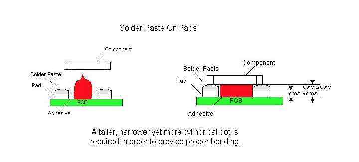
higher profile dot that exhibits very little slump. This will allow the
glue to contact the component, above the height of the solder paste
deposition, when the component is placed. Dots dispensed for this type
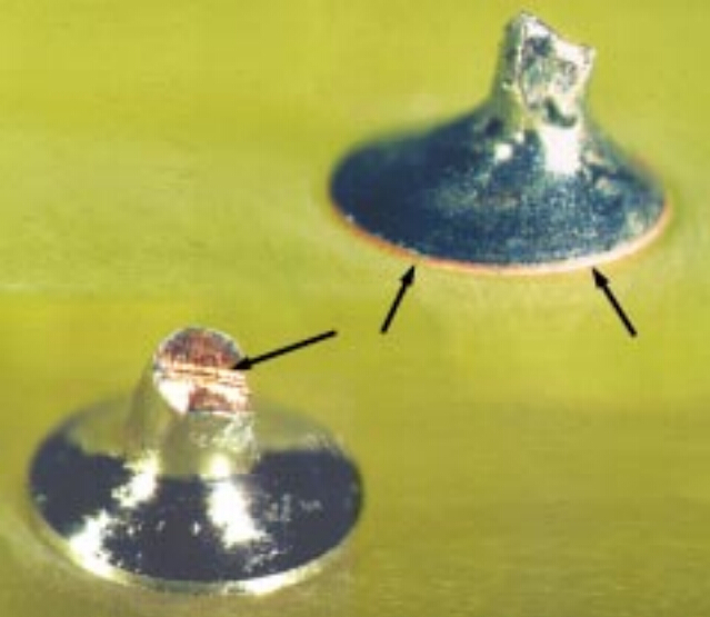
of application should have a tall, cylindrical shape as opposed to the
typical triangular Hershey kiss dot profile. The typical profile may
not allow the glue to properly adhere to the component prior to curing
and then hold the component through wave soldering. This will cause a
large number of missing component errors to be seen following the wave
soldering operation. Excessive missing components following manual
assembly may also be seen because the glue joint is not large enough to
provide the strength needed to hold the components in place.

 The surface mount
adhesive chosen for these applications must also have a high green
strength in order to hold the component prior to the curing process. It
is this green strength that also helps the adhesive to maintain the
tall cylindrical dot shape needed when dispensing between solder pasted
pads. Without it the adhesive deposit will slump, losing contact area
with the component, and causing a decrease in the strength of the
adhesive joints.

SMT,THT,PCB,PCBA,AI,wave soldering,reflow oven,nozzle,feeder,wave soldering,PCB Assembly, LED, LED lamp, LED display,


 In adhesive
dispensing processes utilizing heat, it is difficult to achieve the
necessary dot height. By applying heat to the adhesive, the material’s
viscosity is lowered, allowing it to flow more easily. This type of
flow characteristic will cause the adhesive dot to slump after
dispensing. Problems related to the adhesive not contacting the
component (missing components after wave soldering, etc.) will increase
in frequency, as well as the number of opportunities for defects such as
pad contamination to occur.


Board Design

SMT,THT,PCB,PCBA,AI,wave soldering,reflow oven,nozzle,feeder,wave soldering,PCB Assembly, LED, LED lamp, LED display,


 Typically,
surface mount component pads are designed for either adhesive deposition
or the screening of solderpaste. The pad spacing is generally smaller
for solderpaste application as opposed to that of adhesive deposition.
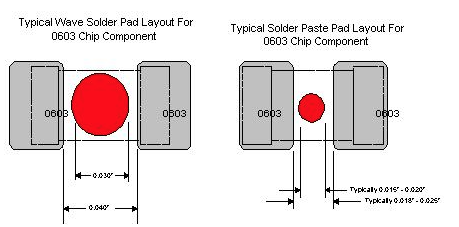
For example, the component pad spacing between the pads of a 0603 chip
cap/resistor is typically 0.020”, if the board was designed to be screen
printed with solderpaste. The pad spacing for the same board can be
0.040” if adhesive deposition was to be utilized. A 0.030” diameter dot
of adhesive would easily be recommended for use if the component pads
on the board were indeed designed for adhesive deposition. However, if
the pad design for the same board was originally designed for
utilization of solderpaste, as a method of adhering the component to the
board, obviously, an 0.030” diameter dot of adhesive would be too
large, as the spacing between the pads is now 0.020”. A 0.015” to 0.018”
diameter dot is required for this particular application.

 In designing pad
spacing and component spacing, the height of the pad and the solder
paste deposition must also be taken into consideration. Typically, the
height of an adhesive dot is one half the diameter of the dot.
Depending upon the material used for the pads, it would be possible
design a board which would be impossible to print and dispense adhesive
on. If the typical dot size for a 0603 component were 0.015” to 0.018”,
the height would be approximately 0.0075” to 0.009”. If the thickness
of the stencil utilized to print the solder paste was 0.006” to 0.007”
this might not allow the glue dot to contact the component body on some
types of board finishes. For example, a typical HASL finish is
approximately 0.003” thick. If the thickness of the stencil utilized
were 0.007”, the adhesive dot would have to be at least 0.011” to 0.012”
tall to properly contact the component. This would require
approximately a 0.022” diameter dot. This is why the rheology of the
adhesive is so important. If the adhesive slumps at all after
dispensing, it may not properly contact the component. The nozzle
design also plays a part in the development of the correct dot for each
application.


Nozzle Design


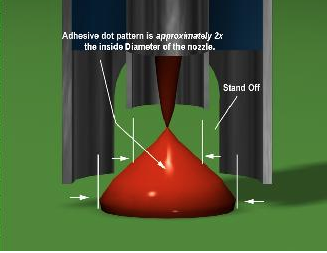
When selecting a nozzle for use in dispensing adhesives the main characteristics that must be considered are nozzle
design, standoff size and placement, and nozzle ID. A relationship
exists between these characteristics and the adhesive dot diameter.
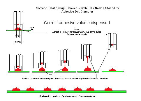
When the adhesive volume is dispensed, the surface tension of the
adhesive on the board, should be twice that of the surface area of the
adhesive at the nozzle tip. If this condition exists, as the nozzle
retracts, the adhesive will snap off clean from the nozzle and leave a
well-defined dot of constant volume on the board. The nozzle must be
chosen based upon the size dot that is required by the application.

SMT,THT,PCB,PCBA,AI,wave soldering,reflow oven,nozzle,feeder,wave soldering,PCB Assembly, LED, LED lamp, LED display,


Nozzle selection
refers in this case to specific nozzle specifications for a known dot
size requirement. The dot size requirements can be derived from the
board design being utilized or specifically the pad spacing of
components. Reference pad spacing previously discussed in this paper. It
is not uncommon for Manufacturing Engineer personnel or Quality
Engineering personnel of a printed circuit board manufacturing facility,
to inquire what a recommended adhesive dot diameter should be for a
particular component type. Much has been written in regards to
recommended surface mount component pad designs and layouts for bottom
side applications. Topside pad designs are also used on bottom side PCB
fabrication. However these guidelines are rarely utilized. The pad
spacing for a particular component for each individual customer product
is unique.

Because the pad
spacing for most typical surface mount components is not standardized
from one customer product to another, it becomes a challenging task when
recommending what tooling should be utilized to satisfy a particular
customers’ adhesive deposition requirement for a particular component.

Note that the
volume of adhesive needed to maintain the component in place during the
high speed placement or wave solder process may be larger than possible
for some specific pad designs.

The nozzle standoff
can be defined as the distance from the tip of the dispensing surface
to the end of the mechanical standoff. The nozzle standoff is used to
maintain the distance between the PCB and the dispensing tip. Most
dispensers in use today are designed to utilize some sort of mechanical
standoff with the nozzles. The standoff usually dictates, to some
degree, the height of the dispensed dot

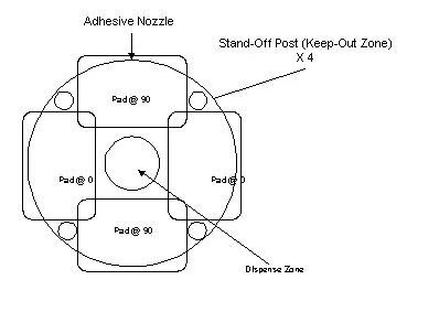
Typical designs for
nozzle standoffs are the castle design, the post design, or a dual post
design. For applications utilizing surface mount adhesive between pads
that have had solder paste applied to them, a single post design nozzle
is the most appropriate. In this type of application the standoff
should be set at 45
° , 135 ° , 215 ° , or 315 ° around the pad circuitry.

SMT,THT,PCB,PCBA,AI,wave soldering,reflow oven,nozzle,feeder,wave soldering,PCB Assembly, LED, LED lamp, LED display, 


When selecting the
correct nozzle ID a rule of thumb is that the nozzle ID should be one
half of the required dot diameter. This will allow for the correct dot
diameter to be dispensed so that the glue snaps away from the nozzle
without contamination. By beginning with this guideline, the
approximate nozzle diameter can be determined, and then adjusted based
upon the material utilized.

SMT,THT,PCB,PCBA,AI,wave soldering,reflow oven,nozzle,feeder,wave soldering,PCB Assembly, LED, LED lamp, LED display,


Stencil Printing Considerations


 When printing
solder paste prior to dispensing surface mount adhesive, there are some
stencil design considerations that must be taken into account. The
thickness of the stencil is important because it will determine the
height of the solder paste depositions. This also determines the
minimum height of the dot that must be dispensed in order to properly
contact and hold the component. In applications where wave soldering
will follow manual assembly, a smaller stencil thickness may be used
because the ultimate solder joint quality will be determined by the wave
soldering operation. It may also be beneficial, on pads with very
tight pads spacing, to undercut the stencil so that as much space as
possible is available for adhesive deposition.


Adhesive Curing


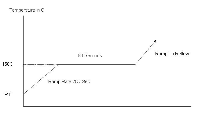
    When printing
solder paste and dispensing epoxy between solder pasted pads a
specialized cure cycle is required. Curing epoxy at 150º C is a
bondline temperature that should be verified with thermocouples at
various locations. Curing epoxy at temperatures above 160º C can cause
the adhesive to become brittle, leading to possible component loss
during the solder wave process. The solution for this is that the epoxy
must be cured at 150º C for about 90 seconds prior to ramping to the
reflow temp. This type of reflow takes into account the adhesive cure
as well as the solder paste reflow. Care should be taken to check the
quality of the solder joints achieved with this profile. The graph
below is a sample of what the cure cycle should look like. The final
profile should take into account the recommended profiles from both the
adhesive and from the solder paste manufacturers.


SMT,THT,PCB,PCBA,AI,wave soldering,reflow oven,nozzle,feeder,wave soldering,PCB Assembly, LED, LED lamp, LED display,


Placement Machine Considerations


 When selecting a
placement machine for use in a process utilizing the dispensing of
surface mount adhesives between solder pasted pads, it is important to
consider the accuracy and the repeatability of the placement machine
down line. In typical top side applications utilizing solder paste
printing, when the solder paste is reflowed, the forces associated with
the solder, automatically center the component, within reason, on its
pads. When glue is added to the process this does not occur because the
glue resists these forces since it is cured prior to the reflowing of
the solder paste. It is important to consider all of the machines in
the line when developing this type of process.


Typical Manufacturing Line Configurations


Traditional Bottom Side Line

SMT,THT,PCB,PCBA,AI,wave soldering,reflow oven,nozzle,feeder,wave soldering,PCB Assembly, LED, LED lamp, LED display,

  GDM Adhesive Dispenser

  Vitronics Reflow Oven

  HSP Chipshooter


Typically, a
traditional bottom side manufacturing line includes an adhesive
dispenser, a chipshooter to place the bottom side components, and an
oven to cure the adhesive. This line will be followed by a wave solder
machine, which will in turn be followed by an inspection and/or rework
station.

The first thing
that must be considered when setting up any manufacturing line is the
type of components and assemblies that are going to be used or built on
it. A traditional bottom side line can be used simply to apply glue to a
printed circuit board, place components on the board, and then cure the
glue in order to hold the parts onto the board prior and during wave
soldering and manual assembly. In this type of application the green
strength of the material determines whether components stay in place
during placement operation on the chipshooter. The post cure strength
of the adhesive determines whether or not the components will stay on
the board during manual assembly and handling. This makes the choice of
glue very important. After wave solder, using this type of line, parts
may be missing due to missing or unacceptable adhesive dots or some may
have be knocked off the board during manual assembly or handling. Care
should be taken to control the forces that these assemblies are
subjected to. This line is very basic in its functionality but can
reliably build products when implemented correctly.


Bottom Side Line With Solder Paste Application

SMT,THT,PCB,PCBA,AI,wave soldering,reflow oven,nozzle,feeder,wave soldering,PCB Assembly, LED, LED lamp, LED display,


  HSP Chipshooter

  DEK Stencil Printer

  Vitronics Reflow Oven

  GDM Adhesive Dispenser


A bottom side line,
that includes solder paste application, incorporates a system for
applying the solder paste (stencil printer or high speed dispenser), an
adhesive dispenser, a chipshooter for the bottom side components, and an
oven to cure the adhesive and reflow the solder paste. A wave solder
machine and an inspection and/or rework station will then follow this
line.

This type of
manufacturing line is more flexible than the previously discussed line.
For bottom side applications, this configuration provides greater torque
strength due to the adhesive being combined with solder paste. This
will assist in reducing the number of missing part defects present in
the assembly. This type of line also helps to reduce problems related
to the wave soldering operation (insufficient solder). In this type of
application, the dot height is important to consider because the dot
must be tall enough to contact the component even above the solder paste
deposit. Consideration also must be given to the design of the stencil
used to print the solder paste and the design of the nozzle used for
high speed dispensing operations. Both of these points can turn into
problems later if not considered properly.


Mixed Technology Top/Bottom Assembly with Solder Paste Application

 SMT,THT,PCB,PCBA,AI,wave soldering,reflow oven,nozzle,feeder,wave soldering,PCB Assembly, LED, LED lamp, LED display,

      Vitronics Reflow Oven

  HSP Chipshooter

  GDM Adhesive Dispenser

  DEK Stencil Printer

  GSM Flexible Placement


A mixed technology
line for assembling top and bottom side products includes a system for
applying the solder paste (stencil printer or high speed dispenser), an
adhesive dispenser, a chipshooter to place the bottom side components, a
flexible placement machine to place top and bottom side components, and
an oven to cure the adhesive and reflow the solder paste. A wave
solder machine and an inspection station will then follow this line.
The inspection station however, should see limited use because of the
robustness of this process.

This manufacturing
line is more flexible than either of the previously discussed lines.
Like the bottom side manufacturing line with solder paste, on bottom
side applications, this configuration provides greater torque strength
due to the adhesive being combined with solder paste. This assists in
reducing the number of missing parts present in the assembly. This
also helps to reduce problems related to the wave soldering operation
(insufficient solder). In this type of application, the dot height is
important to consider because the dot must be tall enough to contact the
component over and above the solder paste deposit. Consideration also
must be given to the design of the stencil used to print the solder
paste and the design of the nozzle used for high speed dispensing
operations. This line also can be used for topside applications
including the deposition of solder paste, chip placement and flexible
placement (QFPs and BGAs for example). This type of flexible
manufacturing line has become the choice for contract electronics
manufacturers because it offers a simple, total assembly solution.


Conclusion


 The dispensing of
surface mount adhesives has been a part of electronics manufacturing
since the development of surface mount components. In an effort to make
the processes involved more robust, solder paste has been added to many
manufacturing line configurations. This configuration helps to
eliminate defects such as missing components and insufficient solder
joints following wave soldering.

 In order to
implement this process there are a lot of considerations that must be
taken into account. The type of adhesive used must have rheological
properties that allow for a tall, cylindrical dot versus the typical
Hershey kiss shaped dot. This type of dot is required to properly
adhere to the component when it is placed on top of the solder paste
deposits. In order to obtain the correct dot height, the board design
must be considered carefully. By designing in the correct pad spacing,
implementation of this process is much simpler. The volume of solder
paste required must then be determined as well as the design of the
stencil. The required adhesive dot size must be considered when
designing the stencil. After the board is designed and the volume of
solder paste required has been determined, a nozzle must be designed to
provide the correct dot diameter with standoffs that will not become
contaminated with solder paste. After the adhesive is deposited and the
chips have been placed, the glue must be cured and the solder paste
must be reflowed. The profile used for this process must be developed
from the adhesive and the solder paste manufacturers’ recommended
profiles. Finally, the type of assemblies that are going to be built
must be considered when developing a manufacturing line that will meet
your needs now and in the future.

 By carefully
considering all aspects of your manufacturing process, the dispensing of
surface mount adhesives between solder pasted pads can help eliminate
defects associated with typical electronics manufacturing processes.
This process helps to eliminate problems such as insufficient solder
joints. In applications where only glue was previously utilized, this
type of process can help eliminate defects such as missing components,
that can occur as a result of handling and manual assembly. By taking
time to consider the characteristics of your manufacturing process, the
correct line configuration and process parameters can be developed to
build the highest quality assemblies possible.


How to evaluate SMT Auto Insertion machine supplier

Quality System Assessment Summary Report

Supplier:  

Commodity Team:

Primary Audit Contact:

Address:     


Supplier Commodity/Product Specialty:

Audit Team:


Phone: 


Fax: 


Elements


Max.

Audit Date:

Re-audit Date:

/ /

%

Improvement


Physical/ Logistical

Capabilities

(for information only)

Score

(0-3)


Score

Score

Score


A. Geographic location

3

1 Management Responsibility


B. Plant condition / size

3

2 Quality System


C. Employment / labor recruiting

2

3 Contract Review


D. Finance resources

3

4 Design Control


E. Pricing history

2

5 Document and Data Control


F.   Equip. Condition /age / application


2

6      Purchasing and verification


G. Backlog / capacity status

2

7 Customer Supplied Products


Yes/ No for following

8 Product Identification and Traceability

4


H. ISO / QS 9000 certified

Yes

9 Process Control


I. Design Capability

Yes

10 Inspection and Testing


J. Quick turn/prototype capability

Yes

11    Control of Inspection and Test Equip.


12


K. JIT capability / Kanban

Yes

12 Inspection and Test Status

2


13 Control of Nonconforming Product


14 Corrective and Preventive Action

6


Calculations:

15 Handling, Storage, Pack. and Delivery

9


1. Quality System Score (%):

16 Control of Quality Records

5


Total Audit Score x 100

17 Internal Auditing

10


(Total Max. Score – N/A Score)

18 Training

6


2. % Improvement:

19 Servicing

4


(New Score – Previous Score) x 100

20 Statistical Techniques

30


Previous Score

21 Continuous Improvements


Total Score


Auditor’s Signature:   


% Score


Date: 

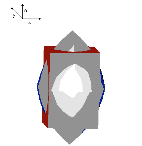
Ball to Pad Coverages for Components with Bumps or Columns

X, Y, θ Space

for square Components With Bumps or Columns

SMT,THT,PCB,PCBA,AI,wave soldering,reflow oven,nozzle,feeder,wave soldering,PCB Assembly, LED, LED lamp, LED display,

Points that lie inside the box represent combinations of x, y, and θ that meet our specs.  

· Points inside the “football” represent combinations that result in 75% feature to pad coverage or better.

· Points that lie inside the box but outside the “football” represent combinations that meet our x, y, and θ specs but yield less than 75% coverage.

· Points that lie inside the “football” but outside the box represent where we are not allowed to operate due to the x, y, and θ specs but would actually give acceptable coverages ( 75%).

· The regions described above (i.e. the portion of the “football” that lies outside the box, etc.) vary in volume depending on the component geometry (span, feature and pad diameters) and the spec. 

Component Programming Tips for SMT pick and place machine

Fiducials and Pad Sites


A
fiducial is a board feature used for global and local error correction
to determine the difference between programmed coordinates and actual
locations on the board. This ensures that parts are not placed before
their locations are verified.


A pad site is a pad pattern on the production board that can be used in the same manner as a fiducial.


The most
typical types of fiducial failures are caused by improper color, size of
fiducial, and lighting values. Other factors such as the confidence
level and search area can also be trouble spots but as the programmer’s
experience level increases, these will be less likely to cause problems.


How many
fiducials to use on a board or circuit will depend on board quality and
the amount of time the manufacturing process can allocate to finding
fiducials. The following is a general guide as to the number of
fiducials used and the benefits of accuracy.


Number of Fiducials Found


Correction Possibilities


1


X and Y


2


X, Y, and Theta


3


X, Y, Theta, and Uniform Stretch


4-5


X, Y, Theta, and Independent X & Y Stretches


6-10 (max)


X, Y, Theta, Independent X & Y Stretches, and Corners not equal to

90 °


The total number of fiducials and pad sites that can be used for a global correction cannot exceed ten.


To use a combination of fiducials and pad sites for global error correction, you must assign them in the Circuit List window.


The total number of fiducials and pad sites that can be used for a local correction cannot exceed five.


To
use a combination of fiducials and pad sites for local error
correction, you must assign them in the Local Fiducials dialog box in
the Placement List window.


When
creating a fiducial or pad site, use the Tab key to move between the
data fields. If you use the Enter key, the fiducial placement is
attempted and error checking is performed.


To successfully create valid fiducial placements:

 –  Fiducials must be placed within the borders of the board.

 –  Fiducials cannot be placed directly on offsets. (Fiducials placed on circuits

   are automatically duplicated on all the offsets associated with that circuit.)

 –  Fiducials cannot be partially on a board or circuit.


If
a fiducial is on an offset and that offset is rotated, the fiducial
location is rotated but the fiducial is not. Only fiducials with
rotational symmetry are supported in this manner. All others will not be
found.


If
multiple fiducial or pad site definitions are selected when using the
Fiducial or Pad Site Copy function, all new fiducials and pad sites are
distanced from the originals by the same X and Y Offset values.


If
fiducials or pad sites are consistently not found by the vision system,
lower the confidence level. If the vision system finds objects other
than the fiducials or pad sites, increase the confidence level.


When
defining a search area, keep in mind that it should be large enough to
allow some tolerance in board handling, but not so large that additional
board features are found instead of the fiducial or pad.


Some recommended lighting levels for fiducials and pad sites.


Fiducial Type / Pad Site


Inner Ring


Outer Ring


Tinned / Tinned


80 / 80


20 / 20

Solder Mask over Bare Copper (not   recommended) / Gold

0 / 0

50 / 35

Bare Copper with Copper Bright / Bare Copper

0 / 0

35 / 35


The pad site functionality is not available for the Odd Form system at this time.


In
most cases, standard lighting cannot be used to image a pad site since
solder paste or flux may not allow a good contrast between the pad site
and the circuit board. Special lighting settings may need to be
installed in order to image the pad site. If Pad Site Find is the only
way to get component corrections, and lighting is the only issue,
consult your UIC Application Engineer.


Use
the Fiducial Lighting procedure located in the Operation Features
Module within the User’s Guide, to determine whether a pad site can be
imaged with the PEC camera. Verify contrast and the lighting level
required.


When to use Pad Site Find

1) When fiducials do not exist on the circuit board

2) When the pad site accurately represents a component type

3) When fiducials do not give an accurate enough correction

4) When accuracy is more important than speed


If
any errors occur finding pad sites, you will be taken to the Fiducial
Repair screen. In the case of failed pad site finds, manual alignment is
not recommended. For GSM1 systems, select the Reject Board button to
remove the board. For GSM2 systems, palm down the machine to manually
remove the board.


The need for a pad site correction is more typical of fine pitch placements such as C4 placements or fine pitch BGA’s.


Pad
sites are based on component definitions. To associate a pad site
definition with a component, the component must be defined in the
database. Refer to the New Component module for information on adding a
component to the database.


PEC Lighting


On
the GSM machine, a Pattern Error Correction (PEC) camera passes an
image to the vision system which attempts to recognize a programmed
fiducial or pad site based on parameters in the Fiducial or Pad Site
List. These parameters consist of type and size, center of fiducial
identified by its “X,Y coordinates”, and the search area identified by
“Search Area X,Y”.


After
the PEC camera moves to the programmed location of the fiducial, it
illuminates the Search Area using the programmed “IN/OUT” (inner
ring/outer ring) light levels. Within the search area of the image,
light intensity differences between the fiducial and the board help the
vision system detect the fiducial’s edges.


The
vision system is able to detect the North, South, East, and West edges
of the fiducials by relying on the differences in contrast between the
board and the fiducial color. Called vector points, triangles of red,
blue, green, and yellow are displayed in the Vision Window.

The
vision system uses six vector points per edge (N, S, E,W). In order for
the vision system to obtain 100% confidence, 24 out of 24 of the vector
points must be detected on an edge of a fiducial. The default
confidence level is 80% (19.2 rounded up to 20 vector points).


Since
the success of fiducial finds depends on the vision system’s ability to
discern the contrast between the board and the fiducial, some
combinations of fiducials (or object(s) to find) and their backgrounds
may call for different types of PEC cameras. Currently 2-sided and
4-sided lighting is being used and FlexLight, a new feature, will soon
be available. The 2-sided PEC camera was non-symmetrical in its lighting
pattern. It illuminated in one direction, from the North and South. The
4-sided PEC camera improved on this by illuminating in four directions,
from the North, South, East, and West. Originally both cameras used red
LED’s. When looking at solder-mask covered fiducials, the red light
would be absorbed by the solder mask (green). To overcome this problem,
green LED’s were added. The 4-sided scheme expanded the capability to
illuminate gold fiducials on white ceramic as well as fiducials on
flexible circuits.


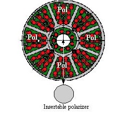
FlexLight (trademark) is an enhanced PEC lighting module. It was originally
developed to address the imaging challenges associated with advanced
substrates such as ceramics and flexible circuits. Although FlexLight
was initially targeted at these markets, it can effectively image a wide
variety of substrate materials ranging from FR-4 to more exotic
materials. The chief advantages of FlexLight are: 1) Symmetric
illumination, 2) Polarization flexibilty,

3) Wavelength flexibility, 4) Ease of reconfiguration, and 5) Monolithic design.


A
mechanical support structure holds eight LED petals and an inner LED
ring. Each petal is a small printed circuit board containing 10 LED’s.
The petals can contain light sources of various wavelengths ranging from
blue to red. The petals and the inner ring can be exchanged in a
“plug-and-play” fashion. This allows the illumination wavelengths of
the module to be quickly and easily changed. It also facilitates ease
of service in the field. The supporting electronics allow the petals to
be configured in various series and parallel combinations to support a
wide variety of LED’s.


The structure supports an optional polarizing film that covers four of the eight petals as shown in the following diagram.

SMT,THT,PCB,PCBA,AI,wave soldering,reflow oven,nozzle,feeder,wave soldering,PCB Assembly, LED, LED lamp, LED display,


Corner Feature Enhancement for Multipattern Components


Multipattern
components consist of components or objects (RF shields, connectors
etc.) which cannot be described adequately as either leaded or leadless
components, but rather are defined in terms of an arrangement of
geometric features. The multipattern object is located by locating each
of the features of which it is comprised, using a single or multiple
fields of view. One such feature, which is commonly used to locate
rectangular or pseudo-rectangular objects, is the corner feature. At
present, this feature is defined simply by entering the length of each
of the two line segments, which make up the 90 degree corner (the
horizontal corner edge length and the vertical corner edge length).
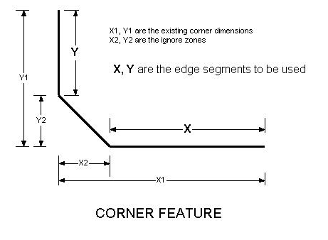
With this special software, this feature definition has been extended to
allow for two more optional parameters. These parameters define
“ignore zones” at the apex of the corner, and allow the image processing
to ignore these regions of the edges when locating the corner. By this
means corners which are rounded, chamfered or poorly defined at the
apex can still be located by using segments of the corner away from the
apex, which subtend 90 degrees to each other.


The diagram below indicates the meaning of each of the parameters.

SMT,THT,PCB,PCBA,AI,wave soldering,reflow oven,nozzle,feeder,wave soldering,PCB Assembly, LED, LED lamp, LED display,


X2, Y2 should not exceed 25% of X1, Y1

If X2 or Y2 = 0, the standard corner find is employed


Enhanced Product Setup


A very helpful feature when programming components is Enhanced Product Setup. It consists of two parts, Enhanced Component Setup
and Enhanced Board Setup. Each process involves a live image, of the
object being taught, to be manipulated while the programmer sees the
changes as they are being made.


When
defining a new component, fill in as many data fields as possible while
paying special attention to the following; Component Height, PreOrient,
Number of Leads, Lighting Type, Camera Type, Default Feeder, Default
Orientation, and Reject Station.


Enhanced Component Setup supports, Four Spindle, C4, OFA (Oddform Assembly) and High Accuracy (UFP) Heads.


If
anything goes wrong with the Platform machine during this entire
process (reject station not mounted, feeder not mounted, exclusion zone,
drop bin not defined, centering fails due to invalid parameter, etc…)
recover by palming the machine down, and up again. Then push the Start
button and proceed to pick the part again.


If
the Platform machine was not calibrated correctly prior to using EPS,
the scale of the drawing may be incorrect and the Draw Component
function cannot be used.


All
changes made are immediately written back to the database scroll list
where the part was defined. Exit the Inspection screen at any time to
view the results of the changes there. Nothing is saved permanently
until the part is saved.


Common ECS Hinderances and Solutions


Before
the part can be picked, all the values associated with component
definition must be entered. This is necessary because these values are
all needed to inspect a component.


All
changes to the drawing are immediately applied to the definition
database of the component. If a mistake is made, rectify the error by
using the Undo function. No change is permanent until the component is
saved.


To
switch from editing the body of the drawing to any of the
leads/bumps/features, click on the leads/bumps/features. To switch back
to editing the body, click where there is no lead/bump/feature.


Due
to the method used for programming leads, it can be difficult to line
up all the leads over their displayed counterparts. This is because
pitches are measured from the center of the side of the component, and
when they are adjusted, leads move symmetrically out or in from/to the
center. To help the adjustment, if there is an odd number of leads,
position the single lead in the center of a side over its corresponding
displayed counterpart. If there is an even number of leads, position the
two center leads over their displayed counterparts before adjusting the
pitch.


To
define a C4 component it is sometimes convenient to define only one
bump initially, and add bumps when the image is displayed, wherever
necessary until the part is found. This is a good procedure because it
may be difficult to determine how bumps will image before seeing an
image of the part.


When
dealing with a large number of leads/bumps at once (over 50), the
drawing function will automatically move only the single lead selected,
instead of all the leads. This is done to increase the performance of
the drawing operations. If less than 50 leads/bumps are selected, they
will all be repositioned at once to give a better indication of their
final positions.


One
of the more difficult things to deal with is when the displayed part’s
rotation is slightly off. Make sure that the feeder pick position is
optimal to present the part accurately. Use the pick/inspect/drop-off
sequence more than once if necessary until the part is basically square
on the screen.


Lead
groups can cause additional problems. The drawing always assumes that
all leads are present on a side, but does not draw some of them if they
were deselected in the leadgroup screen. This can make it difficult for
pitches to be adjusted.


If
the component is too large to fit into a single field of view, the
vision system will take more than one image and stop at the first image
where it could find all leads/bumps/features. This might be the first
image seen, or the last. If the part is found successfully, it will be
the last. This makes editing of the components, by using the Draw
Component function, difficult. Sometimes it is more convenient in this
case to go back and forth between the Database Component Definition
screen and the Inspection screen.


When
viewing a component on the monitor, the image detail may require
enhancement. With the use of Vision Level Diagnostics, the operator can
increase or decrease the detail of the viewed image by raising or
lowering the current vision level. By increasing the Vision Level
Diagnostics to a level 5 setting, the operator can view the image with
the maximum amount of detail. Using a lower vision level results in a
decrease in display detail.


Specific Component Programming


If
a change is necessary while adding a new component to the database, do
not change the component type, exit and begin the procedure again.


The
Accuracy field applies only to a GSM2 (Dual Beam) machine. When the
value is set at high, this means stop the opposite beam while I place
this particular part with the other beam. Our accuracy studies indicate
there is no need to ever run the machine with this value set to high. It
adversely effects throughput and does not contribute to the accuracy of
the machine when placing standard SM devices. Ignore this field for any
other machine configuration.


For
parts that do require a more accurate placement it may be advantageous
to turn on preorient. This indicates to the machine that the part will
be rotated to it’s place rotation prior to being scanned through the
upward looking camera.This allows the machine to minimize the amount of
correction required after being centered and inherently contributes to a
more accurate and repeatable placement. It does however adversely
affect throughtput. Therefore, if you find you the placement accuracy
does not meet your expectation with preorient turned off, turn it on and
reevaluate the accuracy/repeatability of your placements.


When choosing a lighting level for BGA, C4, or C4-Pattern components, a level of +7 should only be used with side-lighting.


C4 Types


The
following restriction applies to programming C4 components on a machine
equipped with an AISI 3500 vision system: A maximum of 16 unique C4
components, with 20 programmed features per component, can be contained
in a product. This restriction is based on the number and type of
programmed C4 features.


Placement
pressure values above 350 grams are typically used for C4 applications.
If the placement head is not C4 capable, these pressures will not be
possible.


The
current bump process is ‘A’, selected as the default. Bump processes
B-E are reserved for future UIC vision inspection algorithms.


The X or Y Vector value will be ignored if the X or Y Number value equals 1.


The % Bumps Required for a C4 component is the percentage of bumps required to return an accurate image.


If
C4-Pattern is not available from the Component Types list box, you must
create a new database. This is done by using the New option under the
Database menu bar heading. If desired, existing component definitions
can then be brought into the new database using the Merge option.


For C4-Pattern, the value for Critical should be chosen as Yes.


There
should be no entry in the Min Precise Patterns, Pattern Inspection,
Location Tolerance X, Location Tolerance Y, or Relative Distance fields.


BGA Types (Requirements and Limitations)


A special version of software is needed, developed after an RFQ, for use with UPS 2.x


The component can only be processed in a single field of view


The appropriate magnification, circular lit camera (circular lit cameras take up 2 additional feeder slots


The vision system must be an AIS630 Lantern vision system only.


The % Bumps Required for a BGA component is the percentage of bumps required simply to display an image.


MISSING BALL DETECTION FOR BGA COMPONENTS


Centering
– the vision system identifies the defined features (bumps) and
determines the x, y, and theta corrections required for an accurate
placement. Bump Process A should be chosen in the component definition.


Inspection
– after the centering process is complete, an additional algorithm is
applied to determine if any bumps are missing. When centering and
inspection are is desired, Bump Process E should be chosen in the
component definition.


This
software inspects BGAs for missing balls using a two step approach.
First the regular ball find algorithm is executed and five candidates
are selected as potential missing ball sites. The selection is based on
either the failure to locate a ball at an expected site, or a low
correlation, or ball recognition score. Then an intelligent pattern
recognition algorithm is trained on sites which are known to contain
good ball images, and the trained algorithm is used to classify the
suspect sites and verify the presence/absence of a solder ball. Various
graphic overlays are used during the execution of the algorithm:


·   It
will be necessary to use circular lighting for bump imaging in order to
realize optimum reliability. This is because the image quality of balls
with the standard lighting is poor.

·   This
algorithm uses a training method based on balls which are found. If
the image quality is such that noise can be incorrectly labeled as a
ball, it is possible to mis-train the algorithm and fail to correctly
identify missing balls.

·   Only components which fit into a single field of view can be processed.

·   In
order to switch on missing ball inspection the customer must select
“processing type E” in the product editor (the default is A). This
processing type flag is provided to allow for customer defined image
processing and in general is not used. It is expected that using this
flag will have no impact on the overall functionality of the machine,
since processing types B-D are still available for customer specific
tuning.

·   This will be a special vision release to support the missing ball inspection.

· The five missing ball candidates are labeled by blue crosses with blue boxes.

· The trained existing balls around the missing ball candidates are labeled by blue crosses only

· The recognized missing ball is labeled by a small red cross on the center of the candidate label


If
the colored graphics are an annoyance, you can change the Vision
Diagnostic Level. The value is probably set at 4 or 5. The range is
between 0-5. The lower the value the faster the machine.


BGA Type

1.4x UPS

Pick and Place

Capable

2.x UPS

Pick and Place

Capable

Special Camera

Requirements

for inspection

Missing Ball

Inspection

Capability

CBGA (ceramic)

Yes

Yes

None

Need Analysis

CCGA, White (ceramic-column)

Yes

Yes

None

No

CCGA, Dark (ceramic-column)

Yes

Yes

None

No

uBGA

Yes

Yes

2.6-3.0 Mil/Pixel Camera

Need Analysis

PBGA (plastic)

Yes

Yes

None

Yes

TBGA (taped)

Yes

Yes

Circular Lighting

No


Camera

Maximum Single Field of View Size

Minimum Pitch

Minimum Ball Diameter

Super High Mag (0.5 mil/pixel)

4mm (0.160”)

0.125mm (0.005”)

0.075mm (0.003”)

High Mag

(1.0 mil/pixel)

10mm (0.39”)

0.25mm (0.010”)

0.125mm (0.005”)

Medium Mag

(2.6 mil/pixel)

20.8mm (0.8”)

0.5mm (0.20”)

0.25mm (0.010”)

Medium Mag

(3.0 mil/pixel)

24mm (0.8”)

0.5mm (0.20”)

0.25mm (0.010”)

Standard Mag

(4.0 mil/pixel)

32mm (1.25”)

0.8mm (0.031”)

0.4mm (0.016”)


Leaded Components


Lead
information must be programmed symmetrically. Information entered for
Sides 1 and 2 of the component is input to Sides 3 and 4, respectively.
The data can then be edited. To accommodate nonsymmetrical components or
components with different lead lengths or pitches, the Lead Groups option may be used.


Lead
groups can cause additional problems. The drawing always assumes that
all leads are present on a side, but does not draw some of them if they
were deselected in the leadgroup screen. This can make it difficult for
pitches to be adjusted.


If
0.0 (zero) is entered in any of the following Tolerance data fields,
that inspection is bypassed; Lead Tolerance From Body, Lead Tolerance
Across Body, Lead Spacing Tolerance, Lead Length Positive Tolerance,
Lead Length Negative Tolerance, Coplanarity Tolerance, and Colinearity
Tolerance.


If
an excessive number of components are rejected, check the component
definition relative to vendor specification sheet for the component.
Also, use ECS (Enhanced Component Setup) to adjust inspection parameters
(geometry, lighting, etc…).


Lead Groups


The
Lead Groups window is not used to toggle leads off for the purpose of
increasing the speed of vision inspection (SMC components only). This
will only result in a rejected component. All components must be defined
as they physically exist. Non-symmetrical leads can be accommodated by
defining the component as a Special-Leaded Component.


Lead
1 in the component database is not necessarily the component’s
electrical pin 1. It is only the first lead in the lower left corner of
the component when the component is in the 0
° orientation. We define/assign leads as beginning with lead one in the
lower left hand corner and count up as we define the part in a
counter-clockwise fashion.


If you select the Remove All Leads option, all component leads are toggled off and considered to be phantom leads. If a lead was already toggled off when the Remove All Leads option was selected, it would remain off.


If
you select the Enable All Leads option, all component leads are toggled
on and are inspected by the vision system. If a lead was already
toggled on when Enable All Leads option was selected, it would remain
on.


Special Leaded Components


Program the component as if all leads on the same side are identical and symmetrical with each other.

When defining a component with different pitches, find the greatest common denominator and enter that as the pitch.


The machine memory supports a maximum of 15 lead groups per component.


When
all lead information is entered, select the Lead Groups option. Select
the leads you want to be ignored by the vision system. The leads are now phantomed with just a broken line to indicate their existence.


Example:

Let’s
use the 23pin SMT connector as an example… There are physically 12
leads on one side of the device and 11 on the opposite side. It would be
a reasonable approach to define both sides as having 23 leads with a
pitch of 1mm, and turning off every other lead in a manner where the
database matches the physical description of the part. However, by
turning off every other lead this creates 23 lead groups, and this is
why the machine hangs up!


We
define/assign leads as beginning with lead one in the lower left hand
corner and count up as we define the part in a counter-clockwise
fashion. For example, for a 14 pin SOIC, lead # 1 is in the lower left
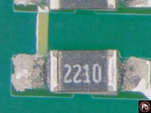
corner and lead # 14 is in the upper left corner (assuming the part is
defined with the leads facing north and south). There are two lead
groups when we define a 14 pin SOIC. Lead group 1 is defined as leads
1-7 and lead group 2 is defined as leads 8-14. However, if you turn off
lead 4 there are now 3 lead groups (lead group 1 = leads 1-3, lead
group 2 = leads 5-7, and lead group 3 = leads 8-14). Notice lead 4 is not included.


By
turning off every other lead you are creating 23 lead groups. We only
have enough RAM on the machine controller to support a maximum of 15
lead groups. However, the number of lead groups is dynamic and can be
limited (reduced) by the number of components, component placements, and
process complexity. Therefore, the number of supported lead groups can
be
£ 15, depending on the product complexity.


Program
the part as it is… Assuming the part is coming in tape and the12
leads are facing 6 O’clock and the 11 leads are facing 12 O’clock, let’s
define the part as having 12 leads on side 1 at a pitch of 2mm and side
3 as having 11 leads at a pitch of 2mm.


Component Terminology


Acronym    Name


BGA      – Ball Grid Array

uBGA      – micro Ball Grid Array

CBGA      – Column Ball Grid Array

C4 or Flip Chip  – Controlled Collapse Chip Connection

COB      – Chip On Board

CSP      – Chip Scale Package

DCA      – Direct Chip Attach

FPT      – Fine Pitch Technology (20 to 40 mil pitch)

ILB      – Inner Lead Bonding

MCM      – Multi Chip Module

MELF      – Metalized ELectrode Face bonded

MSP      – Mini Square Pack

OLB      – Outer Lead Bonding

OMPAC    – Over Molded Plastic pad Array Carrier

PBGA      – Plastic Ball Grid Array

PLCC      – Plastic Leaded Chip Carrier

PQFP      – Plastic Quad Flat Package

QFP      – Quad Flat Package

SOD      – Small Outline Device

SOIC      – Small Outline Integrated Circuit

SOJ      – Small Outline J lead

SOT      – Small Outline Transistor

SQFP      – Shrink Quad Flat Package; QFP with a lead pitch of .016” or less

TAB      – Tape Automated Bonding

TSOP      – Thin Small Outline Package

UFPT      – Ulta Fine Pitch Technology (<20 mil pitch)

V-QFP      – Very Small Quad Flat Package

V-SOP      – Very Small Outline Package


Industry Terms


CER-QUAD    – Digital Equipment Component

C-QUAD    – Northern Telecom Package

Tape Pak    – Trade Mark/National Semiconductor

V-PAK    – Vertical Package (Texas Instruments – memory package)

1


The Barcode Validation System provides a reliable, efficient means of verifying component setup prior to the start of a production run

The Barcode Validation System provides a reliable, efficient means of verifying component setup prior to the start of a
production run 

In an increasing number of circuit board applications, it is important to verify component and feeder
set up prior the start of a production run due to the high cost of post process board repair and
unacceptability of board failure.  It is therfore critical to make sure that the correct components will be
placed before production begins. 


The Barcode Validation System provides the ability to verify that the correct component is in the
correct feeder lane position for a given product, prior to the start of the production run.
Using the Barcode Validation System, feeders are set up and prepared for production off line.  When
the time comes to use these feeders in production, they are mounted to the machine.  At the start of the
production run, the Barode Validation System verifies that each one of these feeders, and their respective
components, has been placed in the correct location before allowing the production sequence to begin. 

FEATURES & BENEFITS 

Component validation process begins with off-line feeder set up, eliminating the need
to check each feeder as it is loaded onto the machine. 

Board production cannot begin until feeder configuration is verified, eliminating the
occurrence of placing the wrong components. 

System can be used with both tape and bulk style feeders, expanding flexibility with
alternative packaging methods. 

Relevant checking and process information is logged for easy report generation and
traceability. 

Barcode Validation System – Features 

The operation of the Barcode Validation System is based on the interaction between the machine’s
internal control system, “smart” component feeders, an off-line bar code scanning system and barcode
labels presented on component reels during feeder set up (see diagram).

Each feeder used in the system is fitted with an electronic  memory tag that is capable of storing data
relevant to the component that is mounted on the feeder.

During the feeder set up operation, typically performed off-line, a feeder is loaded with a reel of
components and placed in a holding fixture.  Next, the barcode(s) on the component reel is scanned
using a hand-held barcode scanner.  Simultaneously, the scanned information is “written”to the
feeder’s memory tag.  All information collected during this process is logged by the BVS system.

Once all feeders for a particular product are set up and ready for production use, they are mounted on
the machine in feeder slots coinciding with the pattern program. 

As the placement sequence begins, the memory tags of all feeders used to build the particular product
are read by the machine’s read/write antennas.  The system then compares this information to the
pattern program data to verify that all relevant components have been loaded into the correct feeder
slots pertaining to the product about to be built.

Once the component configuration has been verified, production begins. 

Southern Machinery WARRANTY POLICY ON ALL NEW Machines

WARRANTY POLICY ON ALL NEW Machines

Southern Machinery warrants its products to be free from defects in materials and workmanship for a period of one year from completion of installation, provided the products are installed as specified by Southern Machinery, maintained by qualified service personnel and the products are operated in accordance with published operating procedures.  For purposes of the foregoing warranties the “completion of installation” shall be that date, within 90 days of shipment of Southern Machinery’s products from its factory, on which the products are installed and operating to the published specifications.  If the customer believes a product to be defective in material or workmanship, or failing to meet the specifications, the customer shall notify Southern Machinery of such alleged defect or failure.  Southern Machinery shall have a reasonable opportunity to investigate any alleged defect or failure, and upon confirmation of its existence Southern Machinery shall promptly remedy the same by repair or replacement, at its discretion and without charge.  The seller warrants parts repaired or replaced for the duration of the original warranty period.

The warranty does not apply to:

1. Consumable parts as they are defined in this document.

or

2. Defects or failures as a result of non-compliance with U Southern Machinery’s installation specifications.

or

3. The customer’s failure to perform the recommended normal maintenance, set up and the adjustment of the equipment.

or

4. The customer’s alteration / modification to the equipment without Southern Machinery’s prior written approval.

or

5. Damages to the equipment resulting from non-compliance with published operating procedures.

or

6. The use of replacement parts not supplied by Southern Machinery or Southern Machinery’s approved suppliers.

Definition of Consumable Parts (Non Warranty):

A) Machine parts that come in direct contact with component processing.

Examples are, but are not limited to, insertion head tooling, chain clips, lead cutter tooling, etc.

B) Maintenance/bulk items.

Examples are, but are not limited to, lubricants, adhesives, light bulbs, fuses, seals, o-rings, etc.

All other machine parts are warranted for 12 months from the machine in-service date, completion of installation.
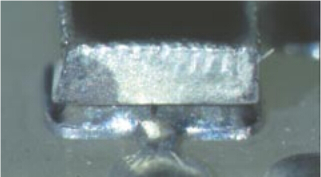
Disclaimer Statement:  

The life expectancy of consumable tooling is dependent on proper preventive maintenance, proper machine set-up, and the type of component used by the customer.  A customer may experience greater life expectancy or less life expectancy depending on the above.