

描述
Product Description
| Specification |
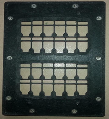
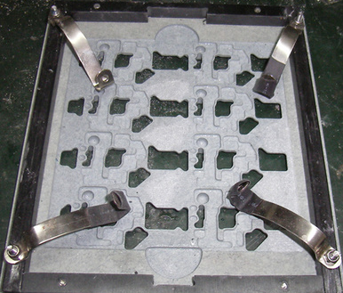
| Item | SMT Fixture For Made In China |
| Surface Treatment | Electro polishing |
| Min.Trace.Spacing | 0.1mm |
| Minimum Line Width |
0.1mm |
|
Minimum Aperture |
0.15mm |
| Overall Thickness |
5mm |
| Copper Thickness | 0.035mm |
| Substrate Material | Synthetic stone |
| Color | Black |
| Size | 14mm* 140mm± 0.1 |
| Outline | Milling |
| Use | Wave soldering |
| Warpage | Less than 2% |
| Lead free | Y |
| Special Process | N |
|
Certificate |
ISO9001; TS16949 |
| OEM And ODM | Welcome |
| Feature |
- Flexible, adapt to a wide range, can greatly shorten production preparation cycle.
- Can save a lot of manpower, material resources, reduce the consumption of the metal material
- It can greatly reduce the storage warehouse area of special fixtures, simplifying administration
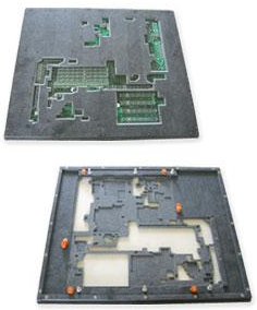
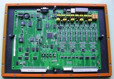
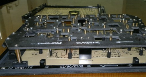
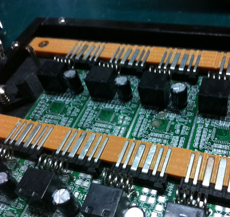
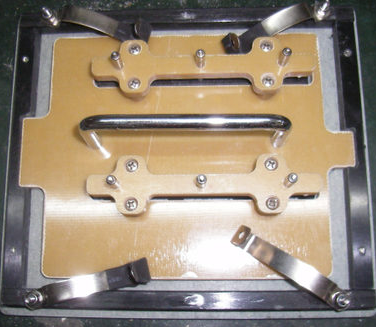
- Tin furnace jig with anti-static synthetic stone material, with high precision, anti-static, high temperature,deformation, low thermal conductivity and other properties, more reliable protection chip devices and PCB board;
- After CNC machining, high precision, chip devices for more effective protection;
- Tin product easy to operate, can be fixed dimensions, the use of a plurality of mold care products to improve production efficiency;
- Single or double cover, for all plug-righting hand, if the missing part of the test role.
| Function |
- Goldfinger avoid contamination
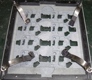
- The SMD soldering surface of the parts covered and protected, leaving only parts fillet DIP tin;
- Prevent PCB bending
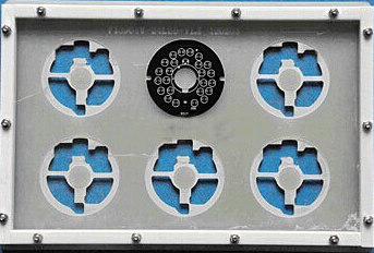
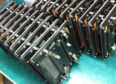
- Use multimode hole design, can carry multiple pieces PCB while the furnace, improve production efficiency can be doubled
- Irregular shape of the PCB Tin necessary
-
Prevent pollution spill tin PCB; 7, can be standardized production line width.


评价
目前还没有评价